|
UNIT – 1 |
||||||||||||
|
INTRODUCTION |
||||||||||||
|
Unit-01/Lecture-01 |
||||||||||||
|
·
Computer Basics and CPU -
Evolution of Computers -
Von Newman model -
CPU -
Memory, I/O -
System Bus -
CPU and Memory registers -
Program Counter -
Accumulator -
Instruction register -
Micro operations -
Register Transfer Language -
Instruction Fetch decode
and execution -
Data movement and
manipulation -
Instruction formats and
addressing modes of basic computer -
8085 microprocessor
organization Evolution of Computers ·
1943: ENIAC (Electronic Numerical Integrator and
Computer) –
Designed and constructed under the direction
Eckert and John Mauchly. –
First general electronic computer. –
It was made up of more than 18000 vacuum tubes
and 1500 relays. –
Primary function was to compute ballistic
trajectories. –
Able to perform nearly 5000 additions or
subtractions per second. –
It was a decimal rather than a binary machine. (or
was it John V. Atanasoff in 1939?) Hard-wired program -- settings of dials
and switches. ·
1944: Beginnings of EDVAC (Electronic Discrete
Variable Computer) –
Among other improvements, includes program stored
in memory. –
John von Neumann and originators of ENIAC
designed the first stored program computer named EDVAC. –
It facilitated the users to enter and alter
various programs and do variety of computations. ·
1945: John von Neumann wrote a report on the
stored program concept, known as the First Draft of a Report on EDVAC. –
The EDVAC project was further developed by Von
Neumann which has now become the usual frame of reference for many modern
computers. Von Newman
model ·
The Von Neumann architecture, also known
as the Von Neumann model and Princeton architecture, is a computer
architecture based on
that described in 1945 by the mathematician and physicist John von Neumann and others in the First Draft of a Report on the EDVAC. · This describes a design architecture for an
electronic digital computer with parts consisting of a processing
unit containing an arithmetic
logic unit and processor
registers, a control unit containing an instruction
register and program counter, a memory to store both data and instructions, external mass storage, and input and output mechanisms. ·
The design
of Von Neumann architecture is simpler than the more modern Harvard
architecture which is
also a stored-program system but has one dedicated set of address and data
buses for reading data from and writing data to memory, and another set of
address and data buses for fetching instructions.
Fig.
Von Neumann Architecture ·
Von Neumann computer systems contain three main
building blocks: o
the central processing unit (CPU), o
memory, o
Input/output devices (I/O). ·
These three components are connected together using the
system bus. ·
The most prominent items within the CPU are the
registers: they can be manipulated directly by a computer program.
Fig.
The following block diagram shows major relationship between CPU
components ·
Components of the Von Neumann
Model
1.
Memory: Storage of information (data/program) 2.
Processing Unit: Computation/Processing of Information 3.
Input: Means of getting information into the computer. e.g.
keyboard, mouse 4.
Output: Means of getting information out of the computer.
e.g. printer, monitor 5.
Control Unit: Makes sure that all the other parts
perform their tasks correctly and at the correct time.
|


|
Unit-01/Lecture-02 |
|
|
The von Neumann Machine:
Fig. Communication between
Memory and Processing Unit
Memory Memory is used to Stores data. All information in computer is stored in binary
form. In the same way we compute memory capacity – in multiples of powers of
2. ·
Communication between memory and processing unit
consists of two registers: o
Memory Address Register (MAR). o
Memory Data Register (MDR). ·
To read, 1.
The address of the location is put in MAR. 2.
The memory is enabled for a read.
3.
The value is put in MDR by the memory. To
write, 1.
The address of the location is put in MAR. 2.
The data is put in MDR. 3.
The Write Enable signal is asserted.
4.
The value in MDR is written to the location specified. ALU, the Processing Unit ·
Processing unit is hardware that implements Arithmetic
and Logical Operations. ·
ALU stands for Arithmetic and Logic Unit,
capable of performing ADD, SUBTRACT, AND, OR, and NOT operations. ·
The size of input quantities of ALU is often referred
to as word length of the computer. ·
Many processors today have word length of 32 and 64
bit. ·
Processing unit also includes a set of registers for temporary storage of data and memory
addressing.
Fig. ALU, The
processing Unit ALU and the Word Length
·
The size of quantities processed by ALU is the word length of the computer. ·
The word length does not affect what a computer can
compute. ·
A computer with a smaller word length can do the same computation as one with a larger
word length but it will take more time. ·
For example, to add two 64 bit numbers, Word
length = 16 takes 4 adds. Word length = 32 takes 2 adds. Word length = 64 takes 1 add.Control Unit
Fig. Control
Unit ·
Control unit includes
Instruction Register IR, Instruction pointer IP (Program counter PC). ·
FSM outputs of the Control
Unit have two purpose: 1.
Control processing that
takes place inside the ALU. 2.
Authorize read/write gate
control of the CPU data path. Input/output
·
The input/output (I/O)
devices interface the computer system with the outside world. ·
These devices allow programs and data to be
entered into the system and provide a means for the system to control some
type of output device. ·
Each I/O port has a unique address to which the CPU
can either read or write a value. ·
From the CPU's point of view, an I/O device
is accessed in a manner very similar to the way it accesses memory. ·
In fact, in some systems the hardware makes
it appear to the CPU that the I/O devices are actually memory locations. ·
I/O controller provides the necessary interface to I/O
devices. ·
Takes care of low-level, device-dependent details. ·
Provides necessary electrical signal interface.
Fig. function of
Input/output device |


|
Unit-01/Lecture-03 |
|
CPU ·
A central
processing unit (CPU) is the electronic
circuitry within a computer that carries out the instructions of a computer program by performing the basic arithmetic,
logical, control and input/output (I/O) operations specified by the
instructions. ·
It referred
to simply as the central processor,
but more commonly called processor, the CPU is
the brains of the computer where most calculations take place. In
terms of computing power, the CPU is the most important element of a computer system. ·
The CPU
itself is an internal component of the computer. Modern CPUs are small and square and
contain multiple metallic connectors or pins on the underside. The CPU is
inserted directly into a CPU socket, pin side down, on the motherboard.
Fig. Central
processing unit (CPU) · It is responsible for controlling the
operations of all other units of a computer system. ALU Performs Arithmetic and logical operations. ·
CU Provides control signals
in accordance with some timing which in turn controls the execution process. • Register Stores data and
result and speeds up the operation. ·
Two typical
components of a CPU are the following: —
The arithmetic logic
unit (ALU), which performs arithmetic and
logical operations. —
The control unit (CU),
which extracts instructions from memory and decodes and executes them, calling on the ALU when necessary.
Fig. Block diagram of a basic uniprocessor-CPU
computer ·
Types
of CPUs
—
There are two main types of CPUs found in computers
today: 32-bit and 64-bit. In addition to this, CPUs can
be broken down into types based on the manufacturer and Memory · The memory unit is a essential
component in a digital computer since it is needed for storing program and data. · The memory unit that communicates directly
with the CPU is called the main memory. ·
Memory is
used to store the information, which includes both program and data. memory refers to the physical devices used to
store programs (sequences of instructions) or data (e.g. program state
information) on a
temporary or permanent basis for use in a computer or other digital electronic device. Memory
Operations
·
There are two key operations on memory: 1.
fetch( address ) returns value without changing the value
stored at that address. 2.
store( address, value ) writes new value into the cell
at the given address. ·
This type of memory is random-access, meaning that CPU can access any
value of the array at any time (vs. sequential access, like on a tape). ·
Such memories are called RAM (random-access memory.) ·
Some memory is non-volatile, or read-only (ROM or read-only memory). Types of Memory (1). Main memory- ·
Memory unit that
communicates directly with the CPU. ·
Static Random Access
Memory–internal flip flops that store the binary information. ·
Dynamic RAM–stores the
binary information in the form of electric charges that are applied to
capacitors. ·
Read Only Memory–store
programs that are permanently resident in the computer and for tables of
constants that do not change in value once the production of the computer is
completed. ·
Bootstrap loader– function
is Start the computer software operating when power is Turned on. ·
Boot Strap program loads a
portion of operating system from disc to main memory and control is then
transferred to operating system. ·
RAM chip – utilizes
bidirectional data bus with three state buffers to perform communication with
CPU. ·
Memory Address map–pictorial
representation of assigned address space for each chip in the system. |


|
Unit-01/Lecture-04 |
|
|
(2). Auxiliary memory ·
Auxiliary memory–devices
that provide backup storage (e.g) magnetic Disks and tapes. Access time-average time required to reach a storage location in
memory and obtain its content. Seek time-time required to position the read/write head to a location. Transfer time- time required to transfer data to or from the device. Transfer rate- No. of characters or words that the device can transfer
per second. (3). Associative memory ·
Associative memory is also called the
Content addressable memory (CAM). ·
CAM is accessed
simultaneously and in parallel on the basis of data content rather than by
specific address or location. ·
Associative memory is more
expensive than a RAM because cell must have storage capability as well as
logic circuits. ·
Argument register-holds an
external argument for content matching. ·
Key-register-mask for
choosing a particular field or key in the argument word.
Fig. Block diagram of associative memory (3). Cache memory- ·
Cache memory–high speed
memory used to increase the speed of processing by making programs and data
available to the CPU at a rapid rate. ·
Locality of
reference-references to memory at any given interval tends to be confined
within a few localized areas of memory. ·
Cache memory-logically
placed between CPU and main memory. ·
Hit-Ratio-ratio of the
number of hits (success in finding the words in cache) to the total CPU
references to memory (hit misses). ·
Mapping-transformation of
data from main memory to cache memory. ·
Current main memory chips
have access times on the order of 60ns to 70ns. When one adds the time it
takes for a memory request to pass from the processor through the system bus
and then the memory controllers and decode logic, the memory access time can
increase to 100ns or more. ·
A processor that runs with a
100MHz clock has a cycle time of 10ns. If we assume that an addition can be
executed in a single processor cycle, then an ADD instruction that takes one
of its operands from main memory might spend 100ns waiting for that operand
and only 10ns doing the addition. The overall time required to complete a
program would then be determined almost entirely by the memory access time;
increasing the processor speed would have very little effect. ·
Caches are introduced into a system to buffer the mismatch between main
memory and processor speeds. A cache is a relatively small, fast memory
placed between the processor and the main memory. The cache is designed so
that its access time matches the processor cycle time. Thus, if the processor
is running with a 100MHz clock the cache should be able to respond to a
memory request in approximately 10ns. In the high-performance single-chip
processors being built today, the cache memory is actually built on the
processor chip and separated into distinct instruction and data caches. The
typical size of these caches is 8kb, for a total of 16kb of cache on the
processor chip. Many system designs also include an off-chip cache, which is
called the second-level cache or the L2 cache:
Fig. Block diagram of Cache Memory · The L2 cache can be anywhere
from 128kb to 4Mb in size. The on-chip cache is called the first-level or
primary cache. While the first-level cache must match the processor speed,
the second-level cache can be somewhat slower than (but not as slow as the
main memory!) · When the processor makes a
memory request, the request first passes to the primary cache. If the data
item is found in this cache, we have a cache hit.
If the data item is not found in the primary cache, we have a cache miss and
the memory request is forwarded to the L2 cache. If the data item is found in
this cache, we have an L2 cache hit and the data is passed back to the
primary cache. If the data is not found in the L2 cache, the request is
finally forwarded to the main memory. When the main memory responds to the
memory request, the data item is passed back to the L2 cache and then the
primary cache. · Caches work well because the
memory request can usually be serviced by the primary cache. In fact,
measurements show that 90% of the time the instruction cache will contain the
requested instruction and 85% of the time the data cache will be able to
respond to the data request. Thus, the L2 and main memory are rarely
accessed. · Typically, the formula for finding the
number of index bits is given only for set associative organizations, because
most authors assume that everyone can remember that fully associative caches
have no index bits and direct mapped enough to reference all slots in the
cache. However, few students seem to get that part. Block Size: Number of bytes per block (in byte-addressable
memory). Used to determine byte offset. Cache Size: Number of bytes in this level of memory
hierarchy. Used with block size to determine number of cache lines,
where each line is associated with one block in cache. We use the termlines
to emphasize the fact that regardless of the number of bytes in the block,
only one tag and validity bit represents the block. Associativity: Types are direct mapped, set associative, and fully associative. Used to
restrict access to cache lines. (4). Virtual memory ·
Virtual memory-permit the
user to construct programs as though large memory space were available, equal
to the totality of the auxiliary memory. ·
An address used by
programmer is Virtual address. ·
Set of Virtual addresses are
called address space. ·
An address in main memory is
called a location or physical address. ·
Set of physical addresses
constitute memory space. ·
Virtual memory can be
organized in different ways. This first scheme is segmentation. ü Segmentation: In segmentation, memory is divided into segments of variable sizes
depending upon the requirements. Main memory segments identified by segments
numbers, start at virtual
address 0, regardless of where they are located in physical memory. In
pure segmented systems, segments are brought into the main memory from the
secondary memory when needed. If segments are modified and not required any
more, they are sent back to secondary memory. This invariably results in gap
between segments, called external fragmentation i.e. less efficient use of
memory. ü Paging: In
this scheme, we have pages of fixed size. In demand paging, pages are
available in secondary memory and are brought into the main memory when
needed. Virtual addresses are formed by concatenating the page number with
the word number. The MMU maps these pages to the pages in the physical memory
and if not present in the physical memory, to the secondary memory.
Fig. Block diagram of Cache Memory |


|
Unit-01/Lecture-05 |
||||||||||||||||
|
System buses ·
A bus is a shared
transmission medium. Must only be used by one device at a time .When used to
connect major computer components (CPU, memory, I/O) is called a system bus. ·
A communication pathway connecting two or more devices. ·
Usually broadcast (all components see signal) ·
Often grouped —
A number of channels in one bus —
e.g. 32 bit data bus is 32 separate single bit channels ·
Power lines may not be shown
Fig. Block
diagram of System Bus Data Bus •
Carries data •
Move data between system
modules. •
Width is a key factor in
determining overall system performance. —
Remember that there is no
difference between “data” and “instruction” at this level •
Width is a key determinant
of performance —
8, 16, 32, 64 bit Address bus •
Identify the source or
destination of data.Means designates source or
destination of data on the data bus. •
Width determines the maximum
possible memory capacity of the system (may be a multiple of width). •
Also used to address I/O
ports. Typically: —
High: Order bits select a
particular module —
Lower: Order bits select a
memory location or I/O port within the module •
e.g. CPU needs to read an
instruction (data) from a given location in memory •
Bus width determines
maximum memory capacity of system —
e.g. 8080 has 16 bit
address bus giving 64k address space Control Bus •
Control and timing
information —
Memory read/write signal —
Interrupt request —
Clock signals ·
Bus Types •
Dedicated —
Separate data &
address lines •
Multiplexed —
Shared lines —
Address valid or data
valid control line —
Advantage - fewer lines —
Disadvantages –
More complex control Ultimate performance ·
Control access to and use of
the data and address lines. ·
It includes: —
Memory Read and Memory Write
—
I/O Read and I/O Write —
Transfer ACK —
Bus Request and Bus Grant —
Interrupt Request and
Interrupt ACK —
Clock —
Reset ·
If one module wishes to send
data to another, it must: — Obtain use of the bus . — Transfer data via the bus . ·
If one module wishes to
request data from another, it must: —
Obtain use of the bus . —
Transfer a request to the
other module over control and address lines —
Wait for second module to
send data. ·
A great number of devices on
a bus will cause performance to suffer . ·
Propagation delay: the time
it takes for devices to coordinate the use of the bus. ·
The bus may become a
bottleneck as the aggregate data transfer demand approaches the capacity of
the bus (in available transfer cycles/second). CPU and
Memory registers ·
Registers
are storage locations internal the the processor. CPU instructions operate on
these values directly. ·
On RISC
processors, all data must be moved into a register before it can be operated. ·
Each
register also has a size that determines the maximum amount of data that can
be processed at a time. The registers on Pentium chips, for example, are 32
bits. Example:
Finally, there are generally only a few registers available on a
processer. Intel chips, for example, have 6 general purpose registers, and
several specialized registers including a base register, stack register,
flags register, program counter, and some addressing registers. ·
Memory, or
RAM, is located external to the CPU. Generally speaking, data has to be
loaded into a CPU register from memory before the CPU can process it, RAM is
much slower than registers, there is a lot more RAM than registers, and
generally memory can be addressed on byte boundaries, where registers may not
be able to access all the bytes in a register. ·
In general,
registers are temporary storage in the CPU that holds the data the processor
is currently working on, while RAM holds the program instructions and the
data the program requires.
Fig. Block
diagram of Register
Memory Registers are memories located within the Central
Processing Unit (CPU). They are few in number (there are rarely more than 64
registers) and also small in size, typically a register is less than 64 bits
in size. The contents of a register can be “read” or
“written” very quickly however, often an order of magnitude faster than main
memory and several orders of magnitude faster than disk memory. Different kinds of register are found within the
CPU. General Purpose Registers are available for general use by the
programmer. Unless the context implies otherwise we’ll use the term
"Register" to refer to a General Purpose Register within the CPU.
Most modern CPU’s have between 16 and 64 General Purpose Registers. Special
Purpose Registers have special uses and are either nonprogrammable and
internal to the CPU or accessed with special instructions by the programmer. Examples of such registers include: ·
Program Counter/Instruction
Pointer Register (PC/IP) ·
Instruction Register (IR) ·
ALU Input & Output Registers ·
Condition Code
(Status/Flags) Register ·
Stack Pointer Register (SP) Although Register Size (the size of the Register
bit-group) tends to vary according to register type, the Word Size of an
Architecture is often (but not always!) defined by the Size of the General
Purpose Registers. In contrast to Main memory and disk memory,
registers are “addressed” directly by specific instructions or by encoding a
register number within a computer instruction. At the programming (assembly)
language level of the CPU, registers are normally specified with special
identifiers (e.g. R0, R1, R7, SP, PC) the contents of a register are lost if
power to the CPU is turned off, so registers are unsuitable for holding
long-term information or information that is needed for retention after a
power-shutdown or failure. Registers are however, the fastest memories, and
if exploited can result in programs that execute very quickly. |
||||||||||||||||
|
Unit-01/Lecture-06 |
||||||||||||||||
|
Program Counter ·
The program
counter (PC), commonly called the instruction pointer (IP) in Intel x86 and Itanium microprocessors, and sometimes called the instruction
address register (IAR) the instruction counter, or just part of
the instruction sequencer, is a processor
register that
indicates where a computer is in its program sequence. ·
It holds
the address of the next instruction to be executed. ·
The program
counter, PC, is a special-purpose register that is used by the processor to
hold the address of the next instruction to be executed. The PLA
automatically updates the PC to point to the next instruction during the
op-code decode cycle. By coordinating with other hardware, in addition to the
PLA, the PC is automatically incremented as each instruction is executed. The
PC can also have an address dictated to it via the 'BRANCH' instruction. ·
Functional
level block diagram of the PC designed for this microprocessor. The PC
possesses the following attributes: outputs an 8-bit address, resets to zero,
can be loaded with any 1 of the possible 256 addresses and produces an
overflow flag if the counter exceeds 256. When the device is reset, via an
external pin, the '/RESET TO ZERO' pin is pulled low by the PLA resulting in
the PC being set to 00h. The PC is incremented by the PLA by pulling the
'/INCREMENT' pin low for 1 clock cycle. If the PC is incremented past its 256
word address reach the 'OVER FLOW FLAG' pin will be driven high. The PC can
be forced to a specified value with the use of the 'BRANCH' command. When the
PLA decodes a 'BRANCH', the PC will latch in the contents of the next 2
addresses. The processor then shifts the concatenated 8-bit address into the
PC.For example if the program counter has the address 305 then the next
instruction will be at location 305 in main memory (RAM). When a program is
running, the program counter will often just be incrementing as it addresses
one instruction after the other, e.g. 305, 306, 307. However, the
instructions will often modify the next address, for example, 305 becomes 39.
What has happened is called a 'jump
instruction'. This is
how the software programmer will cause different parts of his code to run
depending on some condition e.g. a conditional IF statement. It is also how
an interrupt routine is serviced. The program counter will be loaded with the
starting address of the interrupt routine. Accumulator ·
In the central processing unit, or CPU, of a computer, the accumulator
acts as a special register that stores values and increments of intermediate
arithmetic and logic calculations.
The accumulator is a temporary memory location that is accessed speedily by
the CPU. ·
The accumulator is the special
register of the computer. A register is a special memory location that allows
very fast access. Here, the accumulator is a temporary memory location that
stores values of all arithmetic and logical calculations that are being
carried out by the CPU. The increments of values occur in the accumulator for programming
calculations. ·
An
accumulator machine, also
called a 1-operand machine, or a CPU with accumulator-based
architecture, is a kind of
CPU where, although it may have several registers, the CPU mostly stores the
results of calculations in one special register, typically called "the
accumulator". ·
Modern CPUs
are typically 2-operand or 3-operand machines—the additional operands specify
which one of many general
purpose registers (also
called "general purpose accumulators" are used as the source and
destination for calculations. These CPUs are not considered "accumulator
machines". ·
The
characteristic which distinguishes one register as being the accumulator of a
computer
architecture is that
the accumulator (if the architecture were to have one) would be used as an implicit
operand for arithmetic instructions. For instance, a CPU might have an
instruction like: ADD memaddressThis instruction would add the value read from the memory location at memaddress to the value from the accumulator, placing the result in the accumulator. The accumulator is not identified in the instruction by a register number; it is implicit in the instruction and no other register can be specified in the instruction. Some architectures use a particular register as an accumulator in some instructions, but other instructions use register numbers for explicit operand specification.
|
||||||||||||||||
|
Unit-01/Lecture-7 |
||||||||||||||||
|
Instruction
Life Cycle —
Instruction
register a temporary holding ground for the
instruction that has just been fetched from memory. —
In computing, an instruction register (IR) is
the part of a CPU's control unit that stores the instruction currently
being executed or decoded. In simple processors each instruction to be
executed is loaded into the instruction register which holds it while it is
decoded, prepared and ultimately executed, which can take several steps. —
Decoding
the op-code in the instruction register includes
determining the instruction, determining where its operands are in memory,
retrieving the operands from memory, allocating processor resources to
execute the command (in super
scalar processors), etc. —
The output
of IR is available to control circuits which generate the timing signals that
control the various processing elements involved in executing the
instruction. —
In the Instruction
cycle, the instruction is loaded
into the Instruction register after the processor fetches it from the memory
location pointed by the Program counter. —
The
instruction register of a computer stores the current instruction as well as
an address that the instruction will operate on. It is a very simple
component with a very important purpose. —
During the
operation of the computer, the content of a given address in memory is
transferred into the instruction register. —
In my
computer the leftmost four bits are the OP code or current instruction to be
carried out. The right four bits, or lowest four bits, tell the computer what
address to use for the operation. The first four bits constantly feed the OP
code into the control matrix which tells the computer what to do for a given instruction.
The rightmost four bits feed back into the computer so that the address can
be transferred into the MAR or program counter. Instruction cycle ·
An instruction
cycle (sometimes called fetch-and-execute
cycle, fetch-decode-execute
cycle, or FDX) is the
basic operation cycle of a computer. ·
It is the
process by which a computer retrieves a program instruction from its memory, determines what actions the
instruction requires, and carries out those actions. ·
This cycle is repeated continuously by the central processing unit (CPU), from bootup to when the computer is shut
down. ·
In simpler CPUs, the instruction cycle is executed
sequentially: each instruction is completely processed before the next one is
started. ·
In most modern
CPUs, the instruction cycle is instead executed concurrently in parallel, as an instruction
pipeline:
the next instruction starts being processed before the previous instruction
is finished, which is possible because the cycle is broken up into separate
steps.
Fig. Block
diagram of Register
Memory ·
Each computer's CPU can have different cycles based on
different instruction sets, but will be similar to the following cycle: 1.
Fetching the instruction Operation, the PC points to the next instruction that
will be read at the next cycle. 2. Decode the instruction 3 .In case of a memory instruction (direct or indirect)
the execution phase will be in the next clock pulse. If the instruction has
an indirect address, the effective address is read
from main memory, and any required data is fetched from main memory to be
processed and then placed into data registers(Clock Pulse: T3). If
the instruction is direct, nothing is done at this clock pulse. If this is an
I/O instruction or a Register instruction, the operation is performed
(executed) at clock Pulse. 4. Execute the instruction The result generated by the
operation is stored in the main memory, or sent to an output device. Based on
the condition of any feedback from the ALU, Program Counter may be updated to
a different address from which the next instruction will be fetched. The cycle is then repeated. Initiating
the cycle
The cycle starts immediately
when power is applied to the system using an initial PC value that is
predefined for the system architecture (in Intel IA-32 CPUs, for instance, the
predefined PC value is Fetch cycle
Step 1 of the Instruction Cycle
is called the Fetch Cycle. This step is the same for each instruction. 1) The CPU sends PC to the MAR
and sends a READ command on the control bus 2) In response to the read
command (with address equal to PC), the memory returns the data stored at the
memory location indicated by PC on the databus. 3) The CPU copies the data from
the databus into its MDR (also known as MBR (see section Circuits Used above)). 4) A fraction of a second
later, the CPU copies the data from the MDR to the Instruction Register (IR) 5) The PC is incremented so
that it points to the following instruction in memory. This step prepares the
CPU for the next cycle. The Control Unit fetches the
instruction's address from the Memory Unit Decode
Step 2 of the instruction Cycle
is called the Decode Cycle. The decoding process allows the CPU to determine
what instruction is to be performed, so that the CPU can tell how many
operands it needs to fetch in order to perform the instruction. The opcode
fetched from the memory is decoded for the next steps and moved to the
appropriate registers. The decoding is done by the CPU's Control
Unit. Read the effective address
Step 3 is deciding which
operation it is. If this is a Memory operation - in this step the computer
checks if it's a direct or indirect memory operation: ·
Direct memory instruction - Nothing
is being done. ·
Indirect memory instruction -
The effective address is being read from the memory. If this is a I/O or Register
instruction - the computer checks its kind and executes the instruction. Execute cycle
Step 4 of the Instruction Cycle is the Execute Cycle.
Here, the function of the instruction is performed. If the instruction
involves arithmetic or logic, the Arithmetic Logic Unit is utilized. This is
the only stage of the instruction cycle that is useful from the perspective
of the end user. Everything else is overhead required to make the execute
stage happen.
|
||||||||||||||||
|
|
||||||||||||||||
Micro-Operations
·
Micro operations are the basic operations that can be
performed by a system on data stored in registers. Each micro operation
describes a simple operation performed on data in one or more registers. ·
Micro Operations are the
operations which are used to create assembly language instruction. ·
Types of Micro-operation ü Transfer
data between registers ü Transfer
data from register to external ü Transfer
data from external to register ü Perform
arithmetic or logical operations ·
Some common examples of Micro-operation
of Computer Organization are:- — Logical Shift
Right(SHR) —
Logical Shift Left(SHL) b)Circular Shift — Circular
Right(CIR) — Circular
Left(CIL) c)Arithmetic
Shift — Arithmetic Shift
Right(ASHR) — Arithmetic Shift
Left(ASHL) •
A single micro-operation
generally involves a transfer between registers, transfer between registers
and external bus, or a simple ALU operation. •
Each clock
pulse defines a time unit, which are of equal duration. •
Micro-operations are performed within this time unit. •
If multiple
micro-operations do not interfere with one another then grouping of
micro-operations can be performed within one time unit. •
Grouping
can be performed as long as; –
Proper
sequence of events are followed •
PC à MAR must be done first in order for MEMORY
à MDR –
Conflicts
are avoided •
MEMORY à MDR can not be in the same time unit as
MDR à IR System design uses a modular
approach with components at the level of registers, multiplexers, decoders,
adders. Gate level design is generally limited to designing the components,
although some individual gates may be used to connect larger components. Register Transfer Language ·
Micro operations can be expressed in terms of a Register Transfer Language (RTL). ·
A register transfer language is a type of Hardware Description Language (HDL). ·
Since a CPU is a synchronous sequential circuit, micro
operations occur at regular intervals when triggered by the clock pulse. All
sequential circuits in the CPU are generally driven by the same clock in
order to remain in sync. ·
For each clock cycle, zero or more microoperations
occur in the CPU. There is no limit to how many microoperations can occur at
once, provided that no two microoperations require the same circuit to do
different things. Hence, hardware design is somewhat like parallel programming.
·
Digital systems are composed of modules that are
constructed from digital components, such as registers, decoders, arithmetic
elements, and control logic. ·
The modules are interconnected with common data and
control paths to form a digital computer system. ·
The operations executed on data stored in registers are
called microoperations. ·
A micro operation is an elementary operation performed
on the information stored in one or more registers. ·
Examples are shift, count, clear, and load. ·
Some of the digital components from before are
registers that implement microoperations. ·
The symbolic notation used is called a register
transfer language. ·
A programming language is a procedure for writing
symbols to specify a given computational process .
|
||||||||||||||||
|
Unit-01/Lecture-09 |
||||||||||||||||
|
Instruction
formats of basic computer ·
Instruction format defines
the layout of the bits of an instruction, in terms of its constituent
parts. ·
The bits of the instruction
are divided into groups called fields. The most common fields are üAn operation
code that specifies the operation such as add,subtract,multiply etc, to be
performed. üAn address field
that specifies a memory address or register. üA mode field
that tells us how the operand or the effective address of the operand is to
be found out. ·
An instruction consists of
an opcode, usually with some additional information Such as where operands
come from, and where results go. ·
It is the function of the
control unit with in the CPU to interpret each instruction code. ·
The bits of the instruction
are divided into groups called fields. ·
The most common fields are: —
Operation code —
Address field – memory
address or a processor register —
Mode field – specifies the
way the operand or effective address is determined ·
The instructions may have
several different lengths containing varying number of addresses. ·
The number of address fields
in the instruction format of a computer depends on the internal organization
of its registers. ·
Types of instruction formats Various types of instruction formats —
Three address instructions —
Two address instructions —
One address instructions —
Zero address instructions Three address
instructions ·
Three address instructions computer needs three
register address fields. The register address field may be a processor
register or a memory operand. Cyber 170 computer needs three address instructions.
Fig. Three address instructions ADD R1, R2,
R3 The above instruction denotes the operations, R1 <-- R2 + R3 (arithmetic addition) Where R2, R3
= Source registers R1 =
Destination register For Example: ADD R1,
A, B As shown, it is clear that in
the instruction 3 addresses are specified. In the above instruction one
register address and two memory addresses are specified. Example of computer
using this type of instructions Cyber 170. ·
Computers
with three address instructions
formats can use each address field to specify either a processor register or a
memory operand. The program in assembly language that evaluates X= (A+B)*(C+D) is shown below, together with comments that
explain the register transfer operation of each instruction.
Add R2, C, D R2 Mul X, R1,R2 M [X]
It is assumed that the computer has two processor
registers, R1 and R2. The symbol M [A] denotes the operand at memory address
symbolized by A. the advantage of the three
address format
is that it results in short programs when evaluating arithmetic expressions. The disadvantage is that the binary
coded instructions require too many bits to
specify three addresses. An
example of an commercial computer that uses three address instructions is the Cyber 170.The instruction formats in the
Cyber computer are restricted to either three register address fields or two
register address fields and one memory address field. Two address instructions ·
Two
address instructions are the most common in commercial computers. Here again each address field can specify either a processor register or a memory
word.
Fig.
Two address instructions ·
The program to evaluate X= (A+B)*(C+D)
is as follows: MOV R1, A R1 ADD R2, B R1 MOV R2, C R2 ADD R2, D R2 MUL R1, R2 R1 MOV X, R1 M [X] ·
The MOV instruction moves or
transfers the operands to and from memory and processor registers. The
first symbol listed in an instruction is assumed to be both a source and the
destination where the result of the operation is transferred. One address
instructions One address instructions
use an implied accumulator (AC) register for all data manipulation. For multiplication and division there is a need
for a second register. However, here we
will neglect the second register and assume that the AC contains the result
of all operations.
Fig.
One address instructions ·
The program to evaluate X=
(A+B)*(C+D) is LOAD A AC ADD B AC STORE T M [T] LOAD C AC ADD D AC MUL T AC STORE X M [X] All
operations are done between the AC register and a memory operand. T is the
address of a temporary memory location required
for storing the intermediate result.
Commercially available computers also use this type of instruction format. Zero address
instructions A stack organized computer does not use an address field for the
instructions ADD and MUL. The PUSH and POP instructions, however, need an
address field to specify the
operand that communicates with the stack.
Fig. Zero address instructions The following program shows how X=(A+B)*(C+D) will be
written for a stack organized computer.(TOS stands for top of stack.) PUSH A TOS PUSH B TOS ADD TOS PUSH C TOS PUSH D TOS ADD
TOS MUL TOS POP X M[X] To evaluate arithmetic
expressions in a stack computer, it is necessary to convert the expression into reverse polish notation. The name “zero address” is
given to this type of computer because of the absence of an address
field in computational instructions. ·
An instruction format or
instruction code is a group of bits used to perform a particular operation on
the data stored in computer. Processor fetches an instruction from memory and decodes the bits to
execute the instruction. ·
Different computers may have
their own instruction set. ·
In an Instruction format:
First 12 bits (0-11) specify an address.
Next 3 bits specify operation code (opcode).
Left most bit specify the addressing mode I. I=0 for direct
address
15 14
12 11
0
Fig. Instruction format |
||||||||||||||||
|
Unit-01/Lecture-10 |
||||||||||||||||
|
Addressing
modes of basic computer · Addressing modes are an aspect of the instruction set architecture in most central processing unit (CPU) designs. · The various addressing modes
that are defined in a given instruction set architecture define how machine
language
instructions in that architecture identify the operand (or operands) of each
instruction. · An addressing mode specifies
how to calculate the effective memory address of an operand by using
information held in registers and/or constants contained
within a machine instruction or elsewhere. · In computer
programming,
addressing modes are primarily of interest to compiler writers and to those who write
code directly in assembly
language. · Most of the instructions must
refer to the address or content of a specific memory location. These
so-called memory reference instructions must somehow identify the address of
the location as a part of the instruction encoding. · The manner in which this target address or
effective address is identified within the instruction is called the
addressing mode. · Addressing mode refers to the
specification of the location of data required by an operation. · This section describes the more
common addressing modes used in microprocessors: ü Immediate ü Direct ü Indirect ü Register ü Register Indirect ü Displacement (Indexed) ü Stack Immediate Addressing Mode ·
In many cases an instruction
requires a constant quantity, a bit pattern which will never change no matter
when or how often the instruction is executed. This mode includes a bit
pattern as a part of an instruction is called the immediate addressing mode. ·
In Immediate
Addressing mode the operand itself is present in the instruction. It is
generally used for accessing constants.
eg MVI
B , 05 ·
The
advantage of Immediate Addressing mode is that no extra memory reference
needed since the value of the operand is given itself in the instruction. So
Immediate Addressing mode is the fastest addressing mode. ·
The op-word for the
instruction includes a group of bits which identifies this mode of
addressing, and the post-words include the bit pattern itself. ·
Since the instruction is
located in program memory the constant itself is also in program memory. ·
The immediate addressing
mode the instruction does not state explicitly the location of the operand;
rather, it explicitly states the operand itself. ·
Immediate addressing is used when a
particular constant value is to be fixed within the program itself. ·
The value is found in memory
"immediately" after the instruction code word and may never change
at any time. ·
Note that the operand
becomes an integral part of the instruction. ·
The example illustrates this
mode.
Fig. Immediate Addressing Direct Addressing Mode ·
When the instruction
explicitly states the location of an operand or a destination (either in
memory or in a processor register), the addressing mode is known as direct
addressing. ·
The effective address itself
is included in the subsequent words of the instruction (Post-words). ·
Two sub classifications
within the direct addressing mode are often recognized. When the location is
in memory the mode may be referred to as absolute addressing. When the
location is a processor register it may be referred to as register direct
addressing. ·
The
format of Direct Addressing Mode is : Opcode Effective_Address_of_Operand ·
In Direct
Addressing mode the effective address of the operand is given directly in the
instruction. So it requires one extra memory reference to access the operand.
The direct addressing mode is slow compared to immediate addressing
mode. It is generally used to access static variables. ·
Effective
address (EA) = address field (A) e.g. add ax, count or add
ax,[10FC] - Look in memory at address
for operand Figure illustrates the Direct Addressing
Fig. Direct Addressing Indirect Addressing Mode · In the indirect addressing mode the instruction tells the processor
neither the address of the operand nor the operand itself. Instead, it tells
the processor where to go to find the address of the operand. The instruction
may explicitly state either the address of a location in memory or the name of a processor register, but the binary number which is found
there is not the operand. · Instead, it is the effective address, the address of a location in
memory to which the processor must go to find the operand. The result is that
the processor must take one extra step in order to locate the operand. · The op-word for the instruction includes a group of bits which
identifies this mode of addressing, and the (indirect) address is specified
in one or more additional post-words. If the instruction names a processor
register as the source of the effective address, then the register
identification number may fit into the op-word itself. · Indirect addressing is used when a program must operate upon different
data values under different circumstances. · Memory cell pointed to by address field contains the address of
(pointer to) the operand.
EA = (A) —
Look
in A, find address (A) and look there for operand e.g. ADD (A) —
Add
contents of cell pointed to by contents of A to accumulator
Fig. Indirect Addressing Mode Register Addressing Mode · In register addressing, a register,
instead of memory, is used to specify the operand.
This is very similar to direct addressing, except that instead of a memory address,
the address field contains a register reference. The contents of that register
are used as the operand. · Operand(s) is(are) registers EA = R · Register R is EA (not contents of R) · There are a limited number of registers — Therefore a very small
address field is needed — Shorter instructions — Faster instruction fetch — X86: 3 bits used to specify one of
8 registers · No memory access needed to fetch EA · Very fast execution · Very limited address space · Multiple registers can help performance — Requires good assembly
programming or compiler writing — Note: in C you can specify
register variables register int a; — This is only advisory to the
compiler
Fig. Register Addressing Mode |


|
Unit-01/Lecture-11 |
||||||||||||
|
Register Indirect Addressing Modes · In register indirect address mode,
the contents of the designated register are used as a pointer to memory.
Variations of register indirect include the use of post- or pre- increment,
post- or pre- decrement, and displacements. · Register indirect addressing, works exactly the same way as
indirect addressing mode, except it uses a register instead of a memory
address to point to the data. For example, if the instruction is Load R1 and
we are using register indirect addressing mode, we would find the effective
address of the desired operand in R1. · Addressing he operand is held in memory.
The address of the operand location is held in a register which is specified
in instruction. · Useful for accessing different memory locations such as
list of consecutive locations. Contents of register can be incremented after
each access to point to the next location.
Fig. Register Indirect Addressing Modes Displacement (Indexed)
Addressing Modes · In indexed addressing mode, an index
register (either explicitly or implicitly designated) is used to store an
offset (or displacement), which is added to the operand, resulting in the
effective address of the data. · For example, if the operand X of the
instruction Load X is to be addressed using indexed addressing,
assuming R1 is the index register and holds the value 1, and the effective
address of the operand is actually X + 1. Based addressing mode
is similar, except a base address register, rather than an index register, is
used. · In theory, the difference between these two
modes is in how they are used, not how the operands are computed. An index
register holds an index that is used as an offset, relative to the address
given in the address field of the instruction. A base register holds a base
address, where the address field represents a displacement from this base. · These two addressing modes are quite useful
for accessing array elements as well as characters in strings. In fact, most
assembly languages provide special index registers that are implied in many
string operations. Depending on the instruction-set design, general-purpose
registers may also be used in this mode. · Indexed addressing means that the final address for the
data is determined by adding an offset to a base address. · Very often, a chunk of data is stored as a
complete block in memory. For example, it makes sense to store arrays as
contiguous blocks in memory (contiguous means being next to something without
a gap). The array has a 'base address'
which is the location of the first element, then an 'index' is used that adds an offset to
the base address in order to fetch any other element within the array. · Index addressing is fast and is excellent
for manipulating data structures such as arrays as all you need to do is set
up a base address then use the index in your code to access individual
elements. · Another advantage of indexed addressing is
that if the array is re-located in memory at any point then only the base
address needs to be changed. The code making use of the index can remain
exactly the same. · In addition to implementing new
instructions, the extended assembler implements a new addressing mode. This
is indexed addressing, a mode of addressing very useful for arrays.
Here is an example: li $t1,2 # index 2 lb $v0,data($t1) # $v0 = data[$t1] . . . data: .byte 6,34,12,-32, 90 # index zero is first
Think of ·
EA = A + (R) ·
Address field hold two values —
A = base value —
R = register that holds displacement —
or vice versa Fig. Displacement (Indexed) Addressing Modes In Displacement addressing mode the Effective address of the operand
is given by Effective Address = Implicit Processor Register + Displacement The following addressing modes come in the category of Displacement
Addressing mode. ·
Base Addressing mode ·
Index Addressing mode ·
Relative Addressing mode ·
Relative Base Addressing
mode Base Addressing mode: Base addressing mode is used in relocatable programs. Effective
Address =Base Register + Displacement Relative Base Addressing mode: Effective Address = PC + BR + displacement. Where PC stands for
program counter and BR stands for base register. Stack Addressing Modes ·
If stack addressing mode is used, the operand is
assumed to be on the stack. ·
Operand is (implicitly) on top of stack ·
e.g. ADD Pop top
two items from stack and add ·
The stack mode of addressing
is a form of implied addressing ·
The machine instructions need not include a
memory reference but implicitly operate on top of stack. ·
We have noted that it is
desirable to make machine instructions as short as possible. ·
The ultimate limit in
reducing address lengths is having no addresses at all. ·
As we have seen,
zero-address instructions, such as IADD are possible in conjunction with a
stack. ·
It is traditional in mathematics
to put the operator between the operands (x + y), rather than after the
operands (x y +). ·
Between the operands is
called infix notation. After the operands is called postfix or Reverse Polish notation.
Fig. Stack Addressing Modes
|
||||||||||||
|
Unit-01/Lecture-12 |
||||||||||||
|
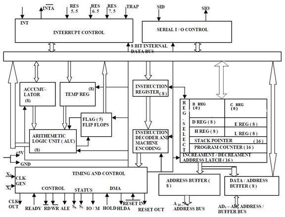
8085 microprocessor organization ·
8085
microprocessor was introduced by Intel in the year 1976. This microprocessor
is an update of 8080 microprocessor. ·
The
8080 processor was updated with Enable/Disable instruction pins and Interrupt
pins to form the 8085 microprocessor. ·
The 8085 is
an 8-bit general purpose microprocessor that can address 64K Byte of memory. It is manufactured with N-MOS technology. ·
It has 16-bit address bus
and hence can address up to 216 = 65536 bytes (64KB) memory locations through
A0-A15. The first 8
lines of address bus and 8 lines of data bus are multiplexed AD0 - AD7. Data
bus is a group of 8 lines D0– D7. ·
It has 40
pins and uses +5V for power. It can run at a maximum frequency of 3 MHz. ·
Basic features of 8085 processor: 8085 microprocessor is an 8-bit microprocessor
with a 40 pin dual in line package. The address and data bus are multiplexed
in this processor which helps in providing more control signals. 8085
microprocessor has 1 Non-maskable interrupt and 3 maskable interrupts. It
provides serial interfacing with serial input data (SID) and serial output
data (SOD): It has a set of registers for
performing various operations. The various registers include · Accumulator (register A) · Registers: B, C, D, E, H and
L · Stack pointer · Program Counter · Temporary register · Instruction register 8085
consists of various units and each unit performs its own functions. The
various units of a microprocessor are listed below ·
Accumulator ·
Arithmetic and logic Unit ·
General purpose register ·
Program counter ·
Stack pointer ·
Temporary register ·
Flags ·
Instruction register and Decoder ·
Timing and Control unit ·
Interrupt control ·
Serial Input/output control ·
Address buffer and Address-Data buffer ·
Address bus and Data bus
Fig.
Internal Architecture of 8085 Microprocessor Accumulator ·
Accumulator is nothing but a register which can hold
8-bit data. Accumulator aids in storing two quantities. ·
The data to be processed by arithmetic and logic unit
is stored in accumulator. ·
It also stores the result of the operation carried out
by the Arithmetic and Logic unit. ·
The accumulator is also called an 8-bit register. The
accumulator is connected to Internal Data bus and ALU (arithmetic and logic
unit). ·
The accumulator can be used to send or receive data
from the Internal Data bus. Arithmetic
and Logic Unit ·
There is always a need to perform arithmetic operations
like +, -, *, / and to perform logical operations like AND, OR, NOT etc. So
there is a necessity for creating a separate unit which can perform such
types of operations. These operations are performed by the Arithmetic and
Logic Unit (ALU). ·
ALU performs these operations on 8-bit data. But these
operations cannot be performed unless we have an input (or) data on which the
desired operation is to be performed. So from where do these inputs reach the
ALU? For this purpose accumulator is used. ALU gets its Input from
accumulator and temporary register. After processing the necessary
operations, the result is stored back in accumulator. General
Purpose Registers ·
Apart from accumulator 8085 consists of six special types
of registers called General Purpose Registers. ·
These general purpose registers are used to hold data
like any other registers. The general purpose registers in 8085 processors
are B, C, D, E, H and L. Each register can hold 8-bit data. Apart from the above
function these registers can also be used to work in pairs to hold 16-bit
data. ·
They can work in pairs such as B-C, D-E and H-L to
store 16-bit data. The H-L pair works as a memory pointer.A memory pointer
holds the address of a particular memory location. They can store 16-bit
address as they work in pair.
Fig. General Purpose Registers Program
Counter ·
Program counter is a special purpose register.
Consider that an instruction is being executed by processor. As soon
as the ALU finished executing the instruction, the processor looks for the
next instruction to be executed. So, there is a necessity for holding the
address of the next instruction to be executed in order to save time. This is
taken care by the program counter. ·
A program counter stores the address of the next
instruction to be executed. In other words the program counter keeps track of
the memory address of the instructions that are being executed by the
microprocessor and the memory address of the next instruction that is going
to be executed. ·
It is a 16 bit register used
as memory pointer. It stores the memory address of the next instruction to be
executed. So we can say that this register is used to sequencing the program.
Generally the memory has 16 bit addresses so that it has 16 bit memory. ·
Microprocessor increments the program whenever an
instruction is being executed, so that the program counter points to the
memory address of the next instruction that is going to be executed. Program
counter is a 16-bit register. Stack pointer · It is also a 16-bit register
which is used as a memory pointer. A stack is nothing but the portion of RAM
(Random access memory). · Stack pointer maintains the
address of the last byte that is entered into stack. Each time when the data is
loaded into stack, Stack pointer gets decremented. Conversely it is
incremented when data is retrieved from stack. · The stack pointer SP, holds the address
of the stack top. The stack is a sequence of memory locations defined by the
programmer. The stack is used to save the content of a register during the
execution of a program. The last memory location of the occupied portion of
the stack is called stack top. For example, suppose that the stack
location 2000 is the stack top which is contained by the stack pointer.
Now the contents of B-C pair so to be saved. This will be stored in the stack
locations 1999 and 1998. The new stack top will be stored in the stack
pointer. The new stack top is the location 1998. If more data come they will
be stored in the stack location 1997 onwards. Suppose the contents of H-L
pair is to be pushed. They will go in 1997 and 1996. The new stack top will
be the stack location 1996 and vacant locations are 1995 onward. Temporary Register: ·
As the name suggests this
register acts as a temporary memory during the arithmetic and logical
operations. Unlike other registers, this temporary register can only be
accessed by the microprocessor and it is completely inaccessible to
programmers. Temporary register is an 8-bit register. Flags ·
The 8085 includes five
flip-flops, also called flags, which are set or reset after an operation
according to data conditions of the result in the accumulator and other
registers. ·
They are called Zero (Z); carry (CY),
Sign(S), Parity (P) and Auxiliary Carry (AC) flags. And
the most commonly used flags are Zero, Carry, and Sign. The 8085 uses these
flags to test data conditions. ·
These flags have critical
importance in the decision-making process of the 8085 simulator. The
conditions (set or reset) of the flags are tested through software
instructions. ·
For example, the instruction
JC (Jump on Carry) is implemented to change the sequence of a program
when the CY flag is set. A good understanding about these five flags is
essential in writing assembly language programs. ·
The overall descriptions
about these flags are: 1.
S-Sign flag: After the execution of an arithmetic or logic operation, if the bit
D7 of the result (usually in the accumulator) is 1, the sign flag is set.
This flag is used with signed numbers. In a given byte, if D7 is 1, the
number will be viewed as a negative number, if it is 0, the number will be
considered positive, in arithmetic operations with signed numbers, bit D7 is
reserved for indicating the sign, and the remaining seven bits are used to represent
the magnitude of a number. However, for unsigned numbers, even if bit D7 of a
result is 1 and the flag is set, it does not mean the result is negative. 2.
Z-Zero flag: The zero flag is set if the arithmetic and logical operation results
in 0, and the flag is reset if the result is not 0. This flag is modified by
the results in the accumulator as well as in the other registers. 3.
AC-Auxiliary Carry flag: In an arithmetic operation, when a carry is generated by digit D3
and passed to digit D4, the AC flag is set. This flag is used internally for
BCD (binary-coded decimal) operations and is not available for the programmer
to change the sequence of a program with a jump instruction. 4.
P-Parity flag: After an arithmetic or logical operation, if the result has an even
number of 1s, the flag is set. If it has an odd number of 1s, the flag is
reset. 5.
CY-Carry flag: If an arithmetic operation results in a carry, the CY flag is set;
otherwise it is rest. The Carry flag also serves as a borrow flag for
subtraction. The
bit position of the flip flop in flag register is:
Timing And
Control Unit ·
Timing and Control Unit:-It provides timing and control signal to the microprocessor to perform
the various operation. It has three control signal. It controls all external
and internal circuits. It operates with reference to clock signal.It
synchronizes all the data transfers. ·
There are three control
signal: 1. ALE-Airthmetic Latch
Enable, It provides control signal to synchronize the components
of microprocessor. 2. RD- This is active low used for reading operation. 3. WR-This is active low used for writing operation. There are three status signal used in
microprocessor S0, S1 and IO/M. It changes its status according the provided
input to these pins.
Serial Input Output Control-There are two pins in this unit. This unit is used for serial data
communication. Interrupt
Control ·
There
are 6 interrupt pins in this unit. Generally an external hardware
is connected to these pins. These pins provide interrupt signal sent by
external hardware to microprocessor and microprocessor
sends acknowledgement for receiving the interrupt signal. Generally INTA
is used for acknowledgement.
|




|
S.No |
Book |
|
1 |
Morris
Mano: Computer System Architecture, PHI. |
|
2 |
William
Stallings: Computer Organization and Architecture, PHI |