|
UNIT
5 / LECTURE 1 |
|||||||||||||||||||||||||||||||||||||||||||
|
Digital
Logic Families [dec’14(2)] What is a Logic Family? What
are the advantages of creating different Logic Families? Electrical
Characteristics of the IC will be identical. In other words, the
different parameters like Noise Margin, Fan In, Fan Out etc will be
identical. Different ICs belonging
to the same logic families will be compatible with each other. Some
Characteristics we consider for the selection of a particular Logic Family
are:
The
basic Classification of the Logic Families are as follows:
Bipolar
Families:
MOS
Families:
Hybrid
Family:
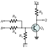
Resistor
Transistor Logic [RTL][jun’14(2)]
Advantage:
UNIT
5/ LECTURE 2
Diode Transistor Logic[DTL]
One way to speed up DTL is to add a small “speed-up”
capacitor across R3. The capacitor helps to turn off the transistor by
removing the stored base charge; the capacitor also helps to turn on the
transistor by increasing the initial base drive
Disadvantage:
TRANSISTOR-TRANSISTOR
LOGIC [TTL] The evolution from DTL to TTL can be seen by observing the
placement of p-n junctions. For example, the diode D2 from Figure 2 in the
chapter on DTL can be replaced by a transistor whose collector is pulled up
to the power supply; transistor Q2 in Figure 1 below. The p-n junction of D2
is replaced by the BE junction of Q2 and with the current gain of the
transistor, the current going into the base of Q3 is greatly increased,
increasing the fanout.
The input diodes and D1 are replaced by the multi-emitter
NPN transistor, Q1, in Fig. 1 and represented by the drawing in Figure 2.
Later on, we will make additional modifications
to this curcuit to improve its performance further. The analysis of this circuit follows very much the same
path as the analysis of the DTL gate.
For the most part, we will consider the input transistor, Q1, to act just
like two diodes. The transistor Q2,
however, will operate in all three regions. The treatment of the output
voltages and currents will be treated the same as the DTL gate and Q3 will
either be cutoff or saturated, corresponding to an output high and an output
low, respectively. ANALYSIS WITH ONE OR MORE INPUTS LOW With an input low, Q3 should be cutoff. We will assume Q2
is cutoff and then check our assumption. If Q2 is cutoff, then there can be
no current coming out of the collector of Q1, hence its base-collector
junction can be modeled as an open circuit.
The base-emitter junction of Q1 will be conducting. The
circuit with these models substituted for the transistors is shown in Figure
3. Note the similarity to the DTL circuit under the same conditions. The two
unused inputs are assumed to be high, and are thus, modeled as open. From
this case, we can see that VoH= 5 volts with no load, and IinL= -I1=
-(5-0.9)/4K = -1.025 mA TTL circuit model with one input low. We turn now to
finding VInLmax. We will use the criterion that Vin will be considered as a
low as long as Q3 is kept cutoff. If the base voltage for Q3 can be raised to
0.5 Volts without turning it on, then there will be 0.5 mA current in the 1KΩ resistor. This
current can only come from Q2, which means it must be conducting. Even
assuming all this 0.5 mA comes through the collector of Q2, the voltage drop
across the 1.4 KΩ resistor will be 0.7 Volts, not enough to cause the
transistor to saturate. Thus, the active model for Q2 is appropriate as shown
in Figure .
TotemPole
Output [june’14(2)] Below is the circuit of TotemPole
NAND-Gate, which has got three stages ·
Input phase ·
Phase splitter
stage ·
Output stage
Advantage
of Totem Pole Outputs The features of this arrangement are ·
Low power
consumption ·
Fast switching ·
Low output
impedance UNIT
5/LECTURE 3
Emitter
Coupled Logic [ECL][jun’14(3)]
Unlike the other logic families in this chapter, ECL does
not produce a large voltage swing between the LOW and HIGH levels. Instead, it has a small voltage swing, less than
a volt, and it internally switches current between two possible paths,
depending on the output state. The first ECL logic family was introduced by General
Electric in 1961. The concept was later refined by Motorola and others to
produce the still popular 10K and 100K ECL families. These families are extremely
fast, offering propagation delays as short as 1 ns. The newest ECL family,
ECLinPS (literally, ECL in picoseconds), offers maximum delays under 0.5 ns
(500 ps), including the signal delay getting on and off of the IC package.
Throughout the evolution of digital circuit technology, some type of ECL has
always been the fastest technology for discrete, packaged logic components.
Figure
: Basic ECL inverter/buffer circuit with input HIGH . Still, commercial ECL families aren’t nearly as popular as
CMOS and TTL, mainly because they consume much more power. In fact, high
power consumption made the design of ECL supercomputers, such as the Cray-1
and Cray-2, as much of a challenge in cooling technology as in digital
design. Also, ECL has a poor speed-power product, does not provide a high
level of integration, has fast edge rates requiring design for
transmission-line effects in most applications, and is not directly
compatible with TTL and CMOS. Nevertheless, ECL still finds its place as a
logic and interface technology in very high-speed communications gear,
including fiber-optic transceiver interfaces for gigabit Ethernet and
Asynchronous Transfer Mode (ATM) networks. When VIN is HIGH, as shown in the figure, transistor Q1 is on, but not saturated, and transistor
Q2 is OFF.
This is true because of a careful choice of resistor values and voltage
levels. Thus, VOUT2 is pulled to 5.0 V (HIGH) through R2, and it can be shown that the voltage drop
across R1is about 0.8 V, so that VOUT1 is about 4.2 V ( LOW).
Figure
ECL Basic ECL inverter/buffer circuit with
input LOW .
Integrated injection logic
Integrated
injection logic (IIL, I2L, or I2L)
is a class of digital circuits built with multiple collector bipolar junction transistors (BJT).[1] When introduced it
had speed comparable to TTL yet was almost as low power as CMOS, making it ideal for use in VLSI (and larger) integrated circuits. Although the logic voltage levels are very close
(High: 0.7V, Low: 0.2V), I2L has high noise immunity because it operates by
current instead of voltage. It is sometimes also known as merged transistor logic.
Simplified
schematic of an I2L inverter. Operation
The
heart of an I2L circuit is the common emitter open collector inverter.
Typically, an inverter consists of an NPN transistor with the emitter
connected to ground and the base biased with a forward current.
The input is supplied to the base as either a current sink (low logic level)
or as a high-z floating condition (high logic level). The output of an
inverter is at the collector. Likewise, it is either a current sink (low logic
level) or a high-z floating condition (high logic level). Like
direct-coupled
transistor logic, there is no resistor between the output (collector) of
one NPN transistor and the input (base) of the following transistor. To
understand how the inverter operates, it is necessary to understand the
current flow. If the bias current is shunted to ground (low logic level), the
transistor turns off and the collector floats (high logic level). If the bias
current is not shunted to ground because the input is high-z (high logic
level), the bias current flows through the transistor to the emitter,
switching on the transistor, and allowing the collector to sink current (low
logic level). Because the output of the inverter can sink current but cannot
source current, it is safe to connect the outputs of multiple inverters
together to form a wired AND gate. When the outputs of two inverters are
wired together, the result is a two-input NOR gate because the configuration
(NOT A) AND (NOT B) is equivalent to NOT (A OR B) (per De
Morgan’s Theorem). Usage
I2L
is relatively simple to construct on an integrated
circuit,
and was commonly used before the advent of CMOS logic
by companies such as Motorola
(now Freescale)[2] and
Texas
Instruments. In 1975, Sinclair
Radionics introduced one of the first consumer-grade digital
watches, the Black
Watch,
which used I2L technology.[3] In
1979, HP introduced a frequency measurement instrument based on a HP-made
custom LSI chip that uses integrated injection logic (I2L) for low
power consumption and high density, enabling portable battery operation,
and also some emitter function logic (EFL) circuits where high speed is
needed.[4] Generally,
I2L gates were constructed with transistors with 1, 2 or 3 separate
collectors. This fan-out of
up to 3 allowed 3-input NAND or NOR
gates to be constructed very simply with just a single layer of interconnect
metal. RCA
used I²L in late 1970s in its CA3162 ADC 3 digit meter.
MOS LOGIC[jun’14(7)]
PMOS logic
P-type metal-oxide-semiconductor logic
uses p-channel metal-oxide-semiconductor field
effect transistors (MOSFETs) to implement logic gates and
other digital
circuits. PMOS transistors operate by creating an inversion
layer
in an n-type
transistor body. This inversion layer, called the p-channel, can conduct holes
between p-type “source”
and “drain” terminals. The
p-channel is created by applying voltage to the third terminal, called the
gate. Like other MOSFETs, PMOS transistors have four modes of operation:
cut-off (or subthreshold), triode, saturation (sometimes called active), and
velocity saturation. The
p-type MOSFETs are arranged in a so-called “pull-up network” (PUN) between
the logic gate output and positive supply voltage, while a resistor is placed
between the logic gate output and the negative supply voltage. The circuit is
designed such that if the desired output is high, then the PUN will be
active, creating a current path between the positive supply and the output. While
PMOS logic is easy to design and manufacture (a MOSFET can be made to operate
as a resistor, so the whole circuit can be made with PMOS FETs), it has
several shortcomings as well. The worst problem is that there is a direct current
(DC) through a PMOS logic gate when the PUN is active, that is, whenever the
output is high, which leads to static power dissipation even when the circuit
sits idle. Also,
PMOS circuits are slow to transition from high to low. When transitioning
from low to high, the transistors provide low resistance, and the capacitative
charge at the output accumulates very quickly (similar to charging a
capacitor through a very low resistance). But the resistance between the
output and the negative supply rail is much greater, so the high-to-low
transition takes longer (similar to discharge of a capacitor through a high
resistance). Using a resistor of lower value will speed up the process but
also increases static power dissipation. Additionally,
the asymmetric input logic levels make PMOS circuits susceptible to noise. Though
initially easier to manufacture, PMOS logic was later supplanted by NMOS logic
because NMOS is faster than PMOS. Modern fabrication uses CMOS,
which uses both PMOS and NMOS transistors together. Static CMOS logic
leverages the advantages of both by using NMOS and PMOS together in the
wafer. We now illustrate the P-channel
MOSFET used as a switch: (a) symbol; (b) circuit model for OFF and ON; (c) P-MOS inverter circuit.
PMOS Inverter The other logic implementations
follow through as for NMOS. Try to figure these out.
NMOS logic
N-type metal-oxide-semiconductor logic
uses n-type
metal-oxide-semiconductor field
effect transistors (MOSFETs) to
implement logic
gates
and other digital
circuits. NMOS transistors have four modes of operation: cut-off
(or sub-threshold), triode, saturation (sometimes called active), and
velocity saturation. The
n-type MOSFETs are arranged in a so-called “pull-down network” (PDN) between
the logic gate output and negative supply voltage, while a resistor is placed
between the logic gate output and the positive supply voltage. The circuit is
designed such that if the desired output is low, then the PDN will be active,
creating a current path between the negative supply and the output. As an example, here is a NOR gate in NMOS logic. If
either input A or input B is high (logic 1, = True), the respective MOS
transistor acts as a very low resistance between the output and the negative
supply, forcing the output to be low (logic 0, = False). When both A and B
are high, both transistors are conductive, creating an even lower resistance
path to ground. The only case where the output is high is when both
transistors are off, which occurs only when both A and B are low, thus
satisfying the truth table of a NOR gate:
A
MOSFET can be made to operate as a resistor, so the whole circuit can be made
with n-channel MOSFETs only. For many years, this made NMOS circuits much
faster than comparable PMOS and CMOS circuits, which had to use much slower
p-channel transistors. It was also easier to manufacture NMOS than CMOS, as
the latter has to implement p-channel transistors in special n-wells on the
p-substrate. The major problem with NMOS (and most other logic families) is
that a DC current must flow through a logic gate even when the output is in a
steady
state
(low in the case of NMOS). This means static power
dissipation, i.e. power drain even when the circuit is not switching.
This is a similar situation to the modern high speed, high density CMOS
circuits (microprocessors etc.) which also has significant static current
draw, although this is due to leakage, not bias. However, older and/or slower
static CMOS circuits used for ASICs, SRAM
etc., typically have very low static power consumption.
Also,
NMOS circuits are slow to transition from low to high. When transitioning
from high to low, the transistors provide low resistance, and the
capacitative charge at the output drains away very quickly (similar to
discharging a capacitor through a very low resistor). But the resistance
between the output and the positive supply rail is much greater, so the low
to high transition takes longer (similar to charging a capacitor through a
high value resistor). Using a resistor of lower value will speed up the
process but also increases static power dissipation. However, a better (and
the most common) way to make the gates faster is to use depletion-mode
transistors instead of enhancement-mode
transistors as loads. This is called depletion-load
NMOS logic. Additionally,
just like in DTL, TTL and
ECL
etc., the asymmetric input logic levels make NMOS circuits somewhat
susceptible to noise. These disadvantages are why the CMOS logic now
has supplanted most of these types in most high-speed digital circuits such
as microprocessors
(despite the fact that CMOS was originally very slow compared to logic gates
built with bipolar
transistors).
CMOS
Logic CMOS or Complementary Metal Oxide Semiconductor logic is
built using both NMOS and PMOS. This comes with several advantages over the
earlier two. CMOS logic is faster and consumes less power. However, it
requires more complex fabrication. Recall that NMOS conducts when its input
is HIGH while PMOS conductswhen its input is LOW. I hope you have read up CMOS characteristics. Take another
look at its physical structure below and then we head straight to the Gates! CMOS Inverter
CMOS Inverter The CMOS inverter is designed to use one NMOS and one
PMOS, both having an equal threshold voltage (in magnitude). Note that the
high and low states correspond to 0 and VDD. Consider the case when VIN =
VDD. Q1 (PMOS) is off while Q2 (NMOS) is on and VOUT = 0. (Note that the PMOS
is the driver circuit). When VIN = 0, Q1 (PMOS) is ON while Q2 (NMOS) is off
. The output VOUT = VDD. Note that in both cases, there is no static current
flowing through the inverter since at any one time; there is no continuous
path to ground. Since the output is an
opposite of the input, this is an inverter. Easy to recall: OFF-
switch open, ON-Switch closed, with the switches modelled by the drain-source
resistance of the respective transistors. CMOS
NAND GATE
CMOS
NOR GATE
Logic
signal voltage levels
Logic
gate circuits are designed to input and output only two types of signals: “high”
(1) and “low” (0), as represented by a variable voltage: full power supply
voltage for a “high” state and zero voltage for a “low” state. In a perfect
world, all logic circuit signals would exist at these extreme voltage limits,
and never deviate from them (i.e., less than full voltage for a “high,” or
more than zero voltage for a “low”). However, in reality, logic signal
voltage levels rarely attain these perfect limits due to stray voltage drops
in the transistor circuitry, and so we must understand the signal level limitations
of gate circuits as they try to interpret signal voltages lying somewhere between
full supply voltage and zero. TTL
gates operate on a nominal power supply voltage of 5 volts, +/- 0.25 volts.
Ideally, a TTL “high” signal would be 5.00 volts exactly, and a TTL “low”
signal 0.00 volts exactly. However, real TTL gate circuits cannot output such
perfect voltage levels, and are designed to accept “high” and “low” signals
deviating substantially from these ideal values. “Acceptable” input signal
voltages range from 0 volts to 0.8 volts for a “low” logic state, and 2 volts
to 5 volts for a “high” logic state. “Acceptable” output signal voltages
(voltage levels guaranteed by the gate manufacturer over a specified range of
load conditions) range from 0 volts to 0.5 volts for a “low” logic state, and
2.7 volts to 5 volts for a “high” logic state:
If a
voltage signal ranging between 0.8 volts and 2 volts were to be sent into the
input of a TTL gate, there would be no certain response from the gate. Such a
signal would be considered uncertain, and no logic gate manufacturer
would guarantee how their gate circuit would interpret such a signal. As you can see, the tolerable ranges for output signal
levels are narrower than for input signal levels, to ensure that any TTL gate
outputting a digital signal into the input of another TTL gate will transmit
voltages acceptable to the receiving gate. The
difference between the tolerable output and input ranges is called the noise
margin of the gate. For TTL gates, the low-level noise margin is the
difference between 0.8 volts and 0.5 volts (0.3 volts), while the high-level
noise margin is the difference between 2.7 volts and 2 volts (0.7 volts).
Simply put, the noise margin is the peak amount of spurious or “noise”
voltage that may be superimposed on a weak gate output voltage signal before
the receiving gate might interpret it wrongly:
CMOS
gate circuits have input and output signal specifications that are quite
different from TTL. For a CMOS gate operating at a power supply voltage of 5
volts, the acceptable input signal voltages range from 0 volts to 1.5 volts
for a “low” logic state, and 3.5 volts to 5 volts for a “high” logic state. “Acceptable”
output signal voltages (voltage levels guaranteed by the gate manufacturer
over a specified range of load conditions) range from 0 volts to 0.05 volts
for a “low” logic state, and 4.95 volts to 5 volts for a “high” logic state:
It
should be obvious from these figures that CMOS gate circuits have far greater
noise margins than TTL: 1.45 volts for CMOS low-level and high-level margins,
versus a maximum of 0.7 volts for TTL. In other words, CMOS circuits can
tolerate over twice the amount of superimposed “noise” voltage on their input
lines before signal interpretation errors will result. CMOS
noise margins widen even further with higher operating voltages. Unlike TTL,
which is restricted to a power supply voltage of 5 volts, CMOS may be powered
by voltages as high as 15 volts (some CMOS circuits as high as 18 volts).
Shown here are the acceptable “high” and “low” states, for both input and
output, of CMOS integrated circuits operating at 10 volts and 15 volts,
respectively:
The
margins for acceptable “high” and “low” signals may be greater than what is
shown in the previous illustrations. What is shown represents “worst-case”
input signal performance, based on manufacturer’s specifications. In
practice, it may be found that a gate circuit will tolerate “high” signals of
considerably less voltage and “low” signals of considerably greater voltage
than those specified here. Conversely,
the extremely small output margins shown – guaranteeing output states for “high”
and “low” signals to within 0.05 volts of the power supply “rails” – are
optimistic. Such “solid” output voltage levels will be true only for
conditions of minimum loading. If the gate is sourcing or sinking substantial
current to a load, the output voltage will not be able to maintain these
optimum levels, due to internal channel resistance of the gate’s final output
MOSFETs. Within
the “uncertain” range for any gate input, there will be some point of
demarcation dividing the gate’s actual “low” input signal range from its
actual “high” input signal range. That is, somewhere between the lowest “high”
signal voltage level and the highest “low” signal voltage level guaranteed by
the gate manufacturer, there is a threshold voltage at which the gate will actually
switch its interpretation of a signal from “low” or “high” or vice versa. For
most gate circuits, this unspecified voltage is a single point:
|