|
UNIT
3 / LECTURE 1 |
||||||||||||||||||||||||||||||||||||||||||||||||||||||||||||||||||||||||||||||||||||||||||||||||||||||||||||||||||||||||||||||||||||||||||||||||||||||||||||||||||||||||||||||||||||||||||||||||||||||||||||||||||||||||||||||||||||||||||||||||||||||||||||||||||||||||||||||||||||||||||||||||||||||||||||||||||||||||||||||||||||||||||||||||||||||||||||||||||||||||||||||||||||||||||||||||||||||||||||||||||||||||||||||||||||||||||||||||||||||||||||||||||||||||||||||||||||||||||||||||||||||||||||||||||||||||||||||||||||||||
Multivibrators
Individual
Sequential
Logic circuits can be used to build more complex circuits
such as Multivibrators, Counters, Shift Registers, Latches and Memories etc,
but for these types of circuits to operate in a “sequential” way, they
require the addition of a clock pulse or timing signal to cause them to
change their state. Clock pulses are generally continuous square or
rectangular shaped waveform that is produced by a single pulse generator
circuit such as a Multivibrator. A multivibrator
circuit oscillates between a “HIGH” state and a “LOW” state producing a
continuous output. Astable multivibrators generally have an even 50% duty
cycle, that is that 50% of the cycle time the output is “HIGH” and the
remaining 50% of the cycle time the output is “OFF”. In other words, the duty
cycle for an astable timing pulse is 1:1. Sequential Logic Circuits that use the clock
signal for synchronization are dependent upon the frequency and clock pulse
width to activate there switching action. Sequential circuits may also change
their state on either the rising or falling edge, or both of the actual clock
signals as we have seen previously with the basic flip-flop circuits. The
following list is terms associated with a timing pulse or waveform. Active
HIGH - if
the state change occurs from a “LOW” to a “HIGH” at the clock’s pulse rising
edge or during the clock width.
Clock Signal Waveform Active LOW - if
the state change occurs from a “HIGH” to a “LOW” at the clock’s pulses
falling edge. Duty Cycle - this
is the ratio of the clock width to the clock period. Clock Width - this
is the time during which the value of the clock signal is equal to a logic
“1”, or HIGH. Clock Period - this
is the time between successive transitions in the same direction, ie, between
two rising or two falling edges. Clock Frequency - the clock frequency is the reciprocal of the clock period, frequency = 1/clock period Clock pulse generation circuits can be a combination of analogue and digital circuits that produce a continuous series of pulses (these are called astable multivibrators) or a pulse of a specific duration (these are called monostable multivibrators). Combining two or more of multivibrators provides generation of a desired pattern of pulses (including pulse width, time between pulses and frequency of pulses). There are basically three types of clock pulse generation circuits:
One way of producing a very simple clock signal is by the interconnection of logic gates. As NAND gates contains amplification, they can also be used to provide a clock signal or timing pulse with the aid of a single Capacitor and a single Resistor to provide the feedback and timing function. These timing circuits are often used because of their simplicity and are also useful if a logic circuit is designed that has unused gates which can be utilized to create the monostable or astable oscillator. This simple type of RC Oscillator network is sometimes called a “Relaxation Oscillator”. ASTABLE MULTIVIBRATOR Transistorized
Astable Multivibrator is a cross coupled transistor network capable of
producing sharp continuous square wave. It is free running oscillator or
simply a regenerative switching circuit using positive feedback. Astable
Multivibrator switches continuously between its two unstable states without
the need for any external triggering. Time period of Astable multivibrator
can be controlled by changing the values of feedback components such as
coupling capacitors and resistors. Circuit diagram of Transistorised Astable Multivibrator
Working principle
At the same time capacitor C2
starts charging through R2, when the C2 voltage exceeds 0.7 V, Q1 turns ON
due to cross coupling. Time Period (T)
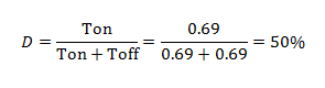
T=Ton + Toff = 0.69 (R1C1+R2C2) Frequency (F)
Duty cycle (D)
UNIT
3 / LECTURE 2
Monostable Multivibrators
Multivibrators
have two different electrical states, an output “HIGH” state and an output
“LOW” state giving them either a stable or quasi-stable state depending upon
the type of multivibrator. One such type of a two state pulse generator
configuration are called Monostable Multivibrators. Monostable Multivibrators have only ONE stable state (hence their
name: “Mono”), and produce a single output pulse when it is triggered
externally. Monostable Multivibrators
only return back to their first original and stable state after a period of
time determined by the time constant of the RC
coupled circuit. In other words, a multi vibrator in which one
transistor is always conducting (i.e. in the ON state) and the other is
non conducting (i.e. in the OFF state) is called mono stable multivibrator.
It is also called a single shot or single swing or a one shot multi vibrator.
Other names are delay multi-vibrator and univibrator. Here we like to describe
Collector
coupled monostable multivibrator
Figure
shows the circuit of a monostable multivibrator using NPN transistor. It
consists of two similar transistor Q1 and Q2 with equal
collector loads i.e. RL1 = RL2 the values of -VBB and
R3 are such as to reverse bias Q1 and keep it at cut
off. The collector supply Vcc and R2 forward bias Q2
and keep it at saturation. A trigger pulse is given through C2 to
obtain the square wave. Initial Conditions:
Let
us suppose that in the absense of a trigger pulse and with S closed,
initially the circuit is in its stable state i.e. Q1 is OFF (at
cut-off) and Q2 is ON (at saturation).
Fig: Monostable Multivibrator When Trigger Pulse is applied
Let
us see as what happens when the trigger is applied.
Return to initial Stable State:
Hence,
the circuit reverts to its original state with Q2 conducting at
saturation and Q1 cur-off. It remains in this state till another
trigger pulse comes along when the entire cycle repeats itself. The
width of duration of the pulse obtained at the collector or output of either
transistor (Q1 or Q2) of the monostable multivibrator
is given by the expression T =
0.69 R2 C1 Emitter
Coupled Monostable Multivibrator
Below
figure shows the circuit diagram of an emitter coupled mono-stable
multi-vibrator.
It
can be observed that the feedback resistive coupling network from the
collector of transistor Q2 to the base of transistor Q1
is absent. instead, the regenerative feedback at the change over from one
state to other is provided by the common emitter resistor REE. The
absence of any coupling from the collector of the transistor Q2
makes it an excellent output point. This has the further advantage of making
the mono stable period independent of any load variation. Further the common
emitter resistor voltage drop VE, Swamps the temperature variation
in VBE, on with temperature and thus makes time period or delay
period stable. Further it is possible to have the voltage controlled delay,
by controlling delay , by controlling the collector current to the transistor
Q1 during quasi-stable state. The collector current of transistor
Q1 can be varied by changing the forward bias of the transistor Q1. The
emitter coupled mono-stable multi-vibrator has the limitation of lower input
voltage. In the normal stable state transistor Q2 is in the
saturation region and transistor Q1 is OFF. On application of an
appropriate trigger pulse, the transistor Q2 starts to work
in the active region reducing the common emitter voltage and forward biasing
the transistor Q1. When transistor Q1 begins to conduct
its collector voltage falls from VCC. This is a negative change
and is transferred by the timing capacitor C, the base of the transistor Q2
reducing the forward bias. Thus both the transistors are in active region and
regenerative feedback ultimately forces transistor Q2 OFF and
transistor Q1 in the ON state, which may be in the active
region of saturation region depending upon the circuit. UNIT
3 / LECTURE 3
The
Bistable Multivibrator [ Dec 2014 (7)]
The Bistable Multivibrator
is another type of two state device similar to the Monostable
Multivibrator we looked at in the previous tutorial but the difference
this time is that BOTH states are stable. Bistable Multivibrators have TWO
stable states (hence the name: “Bi” meaning two) and maintain a given output
state indefinitely unless an external trigger is applied forcing it to change
state. The
bistable multivibrator can be switched over from one stable state to the
other by the application of an external trigger pulse thus, it requires two
external trigger pulses before it returns back to its original state. As
bistable multivibrators have two stable states they are more commonly known
as Latches and
Flip-flops for
use in sequential type circuits. The
discrete Bistable Multivibrator
is a two state non-regenerative device constructed from two cross-coupled
transistors operating as “ON-OFF” Transistor
Switches. In each of the two states, one of the transistors is
cut-off while the other transistor is in saturation, this means that the
bistable circuit is capable of remaining indefinitely in either stable state. Bistable Multivibrator Circuit
fig: Bistable
Multivibrator Circuit To
change the bistable over from one state to the other, the bistable circuit
requires a suitable trigger pulse and to go through a full cycle, two
triggering pulses, one for each stage are required. Its more common name or
term of “flip-flop”
relates to the actual operation of the device, as it “flips” into one logic
state, remains there and then changes or “flops” back into its first original
state. Consider the circuit below. The Bistable
Multivibrator circuit above is stable in both states, either
with one transistor “OFF” and the other “ON” or with the first transistor
“ON” and the second “OFF”. Lets suppose that the switch is in the left
position, position “A”. The base of transistor TR1
will be grounded and in its cut-off region producing an output at Q.
That would mean that transistor TR2 is
“ON” as its base is connected to Vcc through the series combination of
resistors R1 and
R2. As
transistor TR2 is
“ON” there will be zero output at Q, the opposite or
inverse of Q. If
the switch is now move to the right, position “B”, transistor TR2
will switch “OFF” and transistor TR1
will switch “ON” through the combination of resistors R3 and
R4
resulting in an output at Q and zero output at Q the
reverse of above. Then we can say that one stable state exists when
transistor TR1 is
“ON” and TR2 is
“OFF”, switch position “A”, and another stable state exists when transistor TR1 is
“OFF” and TR2 is
“ON”, switch position “B”. Then
unlike the monostable multivibrator whose output is dependent upon the RC
time constant of the feedback components used, the bistable multivibrators
output is dependent upon the application of two individual trigger pulses,
switch position “A” or position “B”. Bistable Multivibrator Waveform
So Bistable
Multivibrators can produce a very short output pulse or a
much longer rectangular shaped output whose leading edge rises in time with
the externally applied trigger pulse and whose trailing edge is dependent
upon a second trigger pulse as shown above. Manually
switching between the two stable states may produce a bistable multivibrator
circuit but is not very practical. One way of toggling between the two states
using just one single trigger pulse is shown below. Sequential Switching Bistable Multivibrator
Switching
between the two states is achieved by applying a single trigger pulse which
in turn will cause the “ON” transistor to turn “OFF” and the “OFF” transistor
to turn “ON” on the negative half of the trigger pulse. The circuit will
switch sequentially by applying a pulse to each base in turn and this is
achieved from a single input trigger pulse using a biased diodes as a
steering circuit. Then
on the application of a first negative pulse switches the state of each
transistor and the application of a second pulse negative pulse resets the
transistors back to their original state acting as a divide-by-two counter.
Equally, we could remove the diodes, capacitors and feedback resistors and
apply individual negative trigger pulses directly to the transistor bases. Bistable
Multivibrators have many applications producing a set-reset, SR
flip-flop circuit for use in counting circuits, or as a one-bit memory
storage device in a computer. Other applications of bistable flip-flops
include frequency dividers because the output pulses have a frequency that
are exactly one half ( ƒ/2 )
that of the trigger input pulse frequency due to them changing state from a
single input pulse. In other words the circuit produces Frequency
Division as it now divides the input frequency by a factor of
two (an octave). UNIT
3/ LECTURE 4
FLIP FLOP A
digital computer needs devices which can store information. A flip flop is a
binary storage device. It can store binary bit either 0 or 1. It has two
stable states HIGH and LOW i.e. 1 and 0. It has the property to remain in one
state indefinitely until it is directed by an input signal to switch over to
the other state. It is also called bistable multivibrator. The
basic formation of flip flop is to store data. They can be used to keep a
record or what value of variable (input, output or intermediate). Flip flop
are also used to exercise control over the functionality of a digital
circuit i.e. change the operation of a circuit depending on the state
of one or more flip flops. These devices are mainly used in situations which
require one or more of these three. Operations,
storage and sequencing. Latch Flip Flop
The
R-S (Reset Set) flip flop is the simplest flip flop of all and easiest to
understand. It is basically a device which has two outputs one output being
the inverse or complement of the other, and two inputs. A pulse on one of the
inputs to take on a particular logical state. The outputs will then remain in
this state until a similar pulse is applied to the other input. The two
inputs are called the Set and Reset input (sometimes called the preset and
clear inputs). Such
flip flop can be made simply by cross coupling two inverting gates either
NAND or NOR gate could be used Figure 1(a) shows on RS flip flop using NAND
gate and Figure 1(b) shows the same circuit using NOR gate.
Fig: Latch R-S Flip Flop Using
NAND Gates To
describe the circuit of Figure 1(a), assume that initially both R and S are
at the logic 1 state and that output is at the logic 0 state. Now,
if Q = 0 and R = 1, then these are the states of inputs of gate B, therefore
the outputs of gate B is at 1 (making it the inverse of Q i.e. 0). The output
of gate B is connected to an input of gate A so if S = 1, both inputs of gate
A are at the logic 1 state. This means that the output of gate A must be 0
(as was originally specified). In other words, the 0 state at Q is
continuously disabling gate B so that any change in R has no effect. Also the
1 state at Now
suppose that the R-S flip flop in the Reset state, the S input goes to 0. The
output of gate A i.e. Q will go to 1 and with Q = 1 and R = 1, the output of
gates B ( There
is another input condition which has not yet been considered. That is when
both the R and S inputs are taken to the logic state 0. When this happens
both Q and
Clocked RS Flip Flop
The
RS latch flip flop required the direct input but no clock. It is very use
full to add clock to control precisely the time at which the flip flop
changes the state of its output. In
the clocked R-S flip flop the appropriate levels applied to their inputs are
blocked till the receipt of a pulse from an other source called clock. The
flip flop changes state only when clock pulse is applied depending upon the
inputs. The basic circuit is shown in Figure . This circuit is formed by
adding two AND gates at inputs to the R-S flip flop. In addition to control
inputs Set (S) and Reset (R), there is a clock input (C) also.
Fig:
Clocked RS Flip Flop
The
excitation table for R-S flip flop is very simply derived as given below
D Flip Flop
A D type (Data or delay flip flop) has a single data input in addition to the clock input as shown in Figure 3.
Fig: D Flip Flop Basically,
such type of flip flop is a modification of clocked RS flip flop gates from a
basic Latch flip flop and NOR gates modify it in to a clock RS flip flop. The
D input goes directly to S input and its complement through NOT gate, is
applied to the R input. This
kind of flip flop prevents the value of D from reaching the output until a
clock pulse occurs. The action of circuit is straight forward as follows. When
the clock is low, both AND gates are disabled, there fore D can change values
with out affecting the value of Q. On the other hand, when the clock is high,
both AND gates are enabled. In this case, Q is forced equal to D when the
clock again goes low, Q retains or stores the last value of D. The truth
table for such a flip flop is as given below in table 6.
The excitation table for D flip flop is very simply derived given as under.
UNIT 3
/LECTURE 5
|
||||||||||||||||||||||||||||||||||||||||||||||||||||||||||||||||||||||||||||||||||||||||||||||||||||||||||||||||||||||||||||||||||||||||||||||||||||||||||||||||||||||||||||||||||||||||||||||||||||||||||||||||||||||||||||||||||||||||||||||||||||||||||||||||||||||||||||||||||||||||||||||||||||||||||||||||||||||||||||||||||||||||||||||||||||||||||||||||||||||||||||||||||||||||||||||||||||||||||||||||||||||||||||||||||||||||||||||||||||||||||||||||||||||||||||||||||||||||||||||||||||||||||||||||||||||||||||||||||||||||




|
Table : The truth table for the JK flip
flop |
|||
|
Initial
Conditions |
Inputs
(Pulsed) |
Final Output |
|
|
Q |
S |
R |
Q (t
+ 1) |
|
0 |
0 |
0 |
0 |
|
0 |
0 |
1 |
0 |
|
0 |
1 |
0 |
1 |
|
0 |
1 |
1 |
1 |
|
1 |
0 |
0 |
1 |
|
1 |
0 |
1 |
0 |
|
1 |
1 |
0 |
1 |
|
1 |
1 |
1 |
0 |
The excitation table for JK flip flop is very
simply derived as given in table 8.
|
Table : Excitation table for JK Flip Flop |
||
|
S |
R |
Q |
|
0 |
0 |
No Change |
|
0 |
1 |
0 |
|
1 |
0 |
0 |
|
1 |
1 |
Toggle |
T Flip
Flop
A
method of avoiding the indeterminate state found in the working of RS flip
flop is to provide only one input ( the T input ) such, flip flop acts as a
toggle switch. Toggle means to change in the previous stage i.e. switch to
opposite state. It can be constructed from clocked RS flip flop be
incorporating feedback from output to input as shown in Figure 5.

Fig:
T Flip Flop
Such
a flip flop is also called toggle flip flop. In such a flip flop a train of
extremely narrow triggers drives the T input each time one of these triggers,
the output of the flip flop changes stage. For instance Q equals 0 just
before the trigger. Then the upper AND gate is enable and the lower AND gate
is disabled. When the trigger arrives, it results in a high S input.
This
sets the Q output to 1. When the next trigger appears at the point T, the
lower AND gate is enabled and the trigger passes through to the R input this
forces the flip flop to reset.
Since
each incoming trigger is alternately changed into the set and reset inputs
the flip flop toggles. It takes two triggers to produce one cycle of the
output waveform. This means the output has half the frequency of the input
stated another way, a T flip flop divides the input frequency by two. Thus
such a circuit is also called a divide by two circuit.
A
disadvantage of the toggle flip flop is that the state of the flip flop after
a trigger pulse has been applied is only known if the previous state is
known. The truth table for a T flip flop is as given table 7.
|
Table
7: Truth table for T Flip Flop |
||
|
Qn |
T |
Qn + 1 |
|
0 |
0 |
0 |
|
0 |
1 |
1 |
|
1 |
0 |
1 |
|
1 |
1 |
0 |
The
excitation table for T flip flop is very simply derived as shown in Table 8.
|
Table
8: Excitation table for T Flip Flop |
|
|
T |
Q |
|
0 |
Qn |
|
1 |
|
Generally
T flip flop ICs are not available. It can be constructed using JK, RS or D
flip flop. Figure 6 shows the relation of T flip flop using JK flip flop.

A D-type
flip flop may be modified by external connection as a T-type stage as shown
in Figure 7. Since the Q logic is used as D-input the opposite of the Q
output is transferred into the stage each clock pulse. Thus the stage having
Q - 0 transistors  = 1, Providing a toggle
action, if the stage had Q = 1 the clock pulse would result in Q = 0 being
transferred, again providing the toggle operation. The D-type flip flop
connected as in Figure 6 will thus operate as a T-type stage, complementing
each clock pulse.
= 1, Providing a toggle
action, if the stage had Q = 1 the clock pulse would result in Q = 0 being
transferred, again providing the toggle operation. The D-type flip flop
connected as in Figure 6 will thus operate as a T-type stage, complementing
each clock pulse.
Master
Slave Flip Flop
Race-Around Condition In J-K Flip Flop[ Dec 2014(2)]
When J=1, K=1, the Q output will be in the Qn’ state after clocking i.e. Qn+1=Qn’. This is known as toggling. The flip flop will complement itself each time the circuit switches from high to low. The flip flop is said to toggle. Practically, we don’t get toggling. Since, clock pulse is more than the propagation delay, so within one clock pulse the output will keep on toggling again and again and it may become indeterminate. This is known as race around condition. Race Around condition occurs because of the feedback connection.
Figure
shows the schematic diagram of master
slave J-K flip flop

Figure
: Master Slave JK Flip Flop
Although
JK Flip-Flop is an improvement on the clocked SR flip-flop it still suffers
from timing problems called “race”
if the output Q changes state before the timing pulse
of the clock input has time to go “OFF”. To avoid this the timing pulse
period ( T ) must be kept as short as
possible (high frequency). As this is sometimes not possible with modern TTL
IC’s the much improved Master-Slave JK Flip-flop was developed.
A
master slave flip flop contains two clocked flip flops. The first is called
master and the second slave. When the clock is high the master is active. The
output of the master is set or reset according to the state of the input. As
the slave is incative during this period its output remains in the previous
state. When clock becomes low the output of the slave flip flop changes
because it become active during low clock period. The final output of master
slave flip flop is the output of the slave flip flop. So the output of master
slave flip flop is available at the end of a clock pulse.
UNIT
3 / LECTURE 6

SHIFT REGISTER [ Dec 2013(2)]
Shift
registers, like counters, are a form of sequential logic. Sequential
logic, unlike combinational logic is not only affected by the present inputs,
but also, by the prior history. In other words, sequential logic remembers
past events.
Shift
registers produce a discrete delay of a digital signal or waveform. A waveform
synchronized to a clock, a repeating square wave, is delayed by "n"
discrete clock times, where "n" is the number of shift
register stages. Thus, a four stage shift register delays "data in"
by four clocks to "data out". The stages in a shift register are delay
stages, typically type "D" Flip-Flops or type "JK"
Flip-flops.
Formerly,
very long (several hundred stages) shift registers served as digital memory.
This obsolete application is reminiscent of the acoustic mercury delay lines
used as early computer memory.
Serial
data transmission, over a distance of meters to kilometers, uses shift
registers to convert parallel data to serial form. Serial data communications
replaces many slow parallel data wires with a single serial high speed
circuit.
Serial
data over shorter distances of tens of centimeters, uses shift registers to
get data into and out of microprocessors. Numerous peripherals, including
analog to digital converters, digital to analog converters, display drivers,
and memory, use shift registers to reduce the amount of wiring in circuit
boards.
Some specialized counter circuits
actually use shift registers to generate repeating waveforms. Longer shift
registers, with the help of feedback generate patterns so long that they look
like random noise, pseudo-noise.
Basic
shift registers are classified by structure according to the following types:
- Serial-in/serial-out
- Parallel-in/serial-out
- Serial-in/parallel-out
- Universal
parallel-in/parallel-out
- Ring counter

Above we show a block diagram of a serial-in/serial-out
shift register, which is 4-stages long. Data at the input will be delayed by
four clock periods from the input to the output of the shift register.
Data at "data in", above, will be present at the
Stage A output after the first
clock pulse. After the second pulse stage A data is transfered to stage B output, and "data in" is transfered to stage A output. After the third clock,
stage C is replaced by stage B; stage B is replaced by stage A;
and stage A is replaced by "data in". After the fourth clock, the
data originally present at "data in" is at stage D, "output". The
"first in" data is "first out" as it is shifted from
"data in" to "data out".

Data is loaded into all stages at once of a
parallel-in/serial-out shift register. The data is then shifted out via
"data out" by clock pulses. Since a 4- stage shift register is
shown above, four clock pulses are required to shift out all of the data. In
the diagram above, stage D data will be present at the "data
out" up until the first clock pulse; stage C data will be present
at "data out" between the first clock and the second clock pulse;
stage B data will be present between the second clock and the third
clock; and stage A data will be present between the third and the
fourth clock. After the fourth clock pulse and thereafter, successive bits of
"data in" should appear at "data out" of the shift
register after a delay of four clock pulses.

If four switches were connected to DA through DD,
the status could be read into a microprocessor using only one data pin and a
clock pin. Since adding more switches would require no additional pins, this
approach looks attractive for many inputs.
Above,
four data bits will be shifted in from "data in" by four clock
pulses and be available at QA through QD for driving
external circuitry such as LEDs, lamps, relay drivers, and horns.
After
the first clock, the data at "data in" appears at QA.
After the second clock, The old QA data appears at QB;
QA receives next data from "data in". After the third
clock, QB data is at QC. After the fourth clock, QC
data is at QD. This stage contains the data first present at
"data in". The shift register should now contain four data bits.

A
parallel-in/parallel-out shift register combines the function of the
parallel-in, serial-out shift register with the function of the serial-in,
parallel-out shift register to yield the universal shift register. The
"do anything" shifter comes at a price– the increased number of I/O
(Input/Output) pins may reduce the number of stages which can be packaged.
Data
presented at DA through DD is parallel loaded into the
registers. This data at QA through QD may be shifted by
the number of pulses presented at the clock input. The shifted data is
available at QA through QD. The "mode" input,
which may be more than one input, controls parallel loading of data from DA
through DD, shifting of data, and the direction of shifting. There
are shift registers which will shift data either left or right.

If
the serial output of a shift register is connected to the serial input, data
can be perpetually shifted around the ring as long as clock pulses are
present. If the output is inverted before being fed back as shown above, we
do not have to worry about loading the initial data into the "ring
counter".
UNIT
3 / LECTURE 7

COUNTERS
Counting
is frequently required in digital computers and other digital systems to
record the number of events occurring in a specified interval of time.
Normally an electronic counter is used for counting the number of pulses
coming at the input line in a specified time period. The counter must possess
memory since it has to remember its past states. As with other sequential
logic circuits counters can be synchronous or asynchronous.
As
the name suggests, it is a circuit which counts. The main purpose of the
counter is to record the number of occurrence of some input. There are many
types of counter both binary and decimal. Commonly used counters are
1.
Binary Ripple Counter
2.
Ring Counter
3.
BCD Counter
4.
Decade counter
5.
Up down Counter
6.
Frequency Counter
Binary Ripple Counter
A
binary ripple counter is generally using bistable multivibrator circuits so
that cache input applied to the counter causes the count to advance or
decrease. A basic counter circuit is shown in Figure 1 using two triggered
(T-type) flip flop stages. Each clock pulse applied to the T-input causes the
stage to toggle. The Q and output terminals are always
logically opposite. If the Q output is logical 1 (SET), the output
is then logical 0. If the Q output is logical 0 (REST), then the output is logical 1.
The
clock input causes the flip flop to toggle or change stage once clock pulse
Figure
2 (a) shows the clock input signal and Q output signal. Notice that the
circuit used in this case toggles on the trailing edge of the clock signal
(when logic signal goes from 1 to 0). Referring back to Figure 1 the Q output
of the first stage (called the 2o stage or units position stage)
is used here as the toggle input to the second stage (called the 21
or two’s position stage). The Q output from the two successive stage are
marked A and B, respectively, to differentiate them. Notice that the output
of each stage is marked with a negative bar over the letter designation, so
that whatever logical stage A is at,  is
the opposite logical state.
is
the opposite logical state.
Since
the Q output (A signal) from the first stage triggers the second stage, the
second stage changes state only when the Q output of first stage goes from
logical 1 to logical 0 as shown in Figure 2(b).

Table
1
|
COUNT FOR 2-STAGE BINARY COUNTER |
||
|
Input Pulses |
2n Output (B) |
2n Output (A) |
|
0 |
0 |
0 |
|
1 |
0 |
1 |
|
2 |
1 |
0 |
|
3 |
1 |
1 |
|
4 or 0 |
0 |
0 |
An arrow is included on the waveform of stage A as a
reminder that it triggers stage B only on a trailing edge (1 or 0 logical
change). Notice that the output waveform of succeeding stage operates half as
fast as its input. To see that this circuit operates as a binary counter a
table can be prepared to show the Q output states after each clock pulse is
applied. Table 1 shows this operation for the circuit of Figure 1.
To see how a counter is made using more stage considers
the 4 stage counter of Figure 3. The counter is simply made with the Q output
of each state connected as the toggle input to the succeeding state. With
four stages the counter cycle will repeat every sixteen clock pulses. In
general there are 2n counts with an n-stage counter. For the four
stages used here the count goes 24 or 16 steps as a rule, for a
binary counter.
Number of counts = N = 2n
Where, n = number of counter stage. A six stage counter n
= 6 would be provide a count that repeats every N = 26 = 64
counts. A ten-stage counter (n = 10) would recycle every N = 210 =
1024 counts.
Returning to the 4 stage counter Figure 3. Arrows
are included in the table to act as reminder that a change from 1 to 0
results in a succeeding stage being toggled. Notice in Table 2 that the 20
stage toggles on every four clock pulses. The 21 stage toggles
every two clock pulses, the 22 stage toggles every clock pulses.
This implies that we can associate a weighting value to the stage output. The
23 stage output can be considered of value eight, the 22
output equal four, 21 output equals two and 20 equals
one. We can see then that the binary state of the counter can be read as a
number equals to the pulses input count. After the counter reaches the count
111, which is the largest count obtained using four stages, the next input
pulse causes the counter to go to 000 and new count cycle repeats.
repeats.

Table
2
|
COUNT UP OPERATION (FOUR STAGES) |
||||
|
Input Pulses |
23Output (D) |
22 Output (C) |
21 Output (B) |
20 Output (A) |
|
0 |
0 |
0 |
0 |
0 |
|
1 |
0 |
0 |
0 |
1 |
|
2 |
0 |
0 |
1 |
0 |
|
3 |
0 |
0 |
1 |
1 |
|
4 |
0 |
1 |
0 |
0 |
|
5 |
0 |
1 |
0 |
1 |
|
6 |
0 |
1 |
1 |
0 |
|
7 |
0 |
1 |
1 |
1 |
|
8 |
1 |
0 |
0 |
0 |
|
9 |
1 |
0 |
0 |
1 |
|
10 |
1 |
0 |
1 |
0 |
|
11 |
1 |
0 |
1 |
1 |
|
12 |
1 |
1 |
0 |
0 |
|
13 |
1 |
1 |
0 |
1 |
|
14 |
1 |
1 |
1 |
0 |
|
15 |
1 |
1 |
1 |
1 |
|
16 or 0 |
0 |
0 |
0 |
0 |

It
should be obvious that the count sequence is an increasing binary count for
each input clock pulse. Then the counter is also referred to as a count up
binary counter the resulting output waveform for each stage is shown in
Figure 4. The count is called a ripple counter because of the rippling change
of state from lower order to higher order stages when the count changes i.e.
the 20 stage toggles the 21 stage, which may toggle the
22 stage etc.
UNIT 3 /LECTURE
8

Count-Down
Counter [DEC 2013(7)]
A
simple four stage countdown counter is shown is Figure 5. The Q-output of
each stage is now used as trigger input to the following stage. It still use
the Q-output as indication the state of each stage as shown in the count
table (table 3). Starting with the counter RESET Q-output of each stage is
logical-0, the first input pulse causes stage A to toggle form 0 to 1. The
trigger pulse to stage B being taken from the Q-output of stage A goes from 1
to 0 at this time so that stage B is also toggled. The Q-output of stage B
going from 1 to 0 causes stage C to be toggled, which then causes stage D to
toggle.

Figure 5: Four Stage Count-down Binary Counter
|
Table
5: Count-down Counter of Figure 5 |
|||||
|
Input
Pulse |
D |
C |
B |
A |
Decimal
Output Count |
|
0 |
0 |
0 |
0 |
0 |
0 (or 16) |
|
1 |
1 |
1 |
1 |
1 |
15 |
|
2 |
1 |
1 |
1 |
0 |
14 |
|
3 |
1 |
1 |
0 |
1 |
13 |
|
4 |
1 |
1 |
0 |
0 |
12 |
|
5 |
1 |
0 |
1 |
1 |
11 |
|
6 |
1 |
0 |
1 |
0 |
10 |
|
7 |
1 |
0 |
0 |
1 |
9 |
|
8 |
1 |
0 |
0 |
0 |
8 |
|
9 |
0 |
1 |
1 |
1 |
7 |
|
10 |
0 |
1 |
1 |
0 |
6 |
|
11 |
0 |
1 |
0 |
1 |
5 |
|
12 |
0 |
1 |
0 |
0 |
4 |
|
13 |
0 |
0 |
0 |
1 |
3 |
|
14 |
0 |
0 |
1 |
0 |
2 |
|
15 |
0 |
0 |
0 |
1 |
1 |
|
16 |
0 |
0 |
0 |
0 |
0 (or 16) |
|
|
1 |
1 |
1 |
1 |
15 |
Table 5 shows, then that the count goes to 1111. The next
input puse toggles A. Since the signal A (used to toggle stage B) now goes
input 0 to 1. Stage B and C and D remain the same, the count now being 1110.
Thus, the count has deceased as a result of the input trigger pulse. In fact
the count will countinue to decrease by one binary count for each input
trigger pulse applied. Table 5 shows that the count will decrease to 0000
after which it will go to 1111 to repeat another count circle. Using four stage
the count down counter provides a full cut off
N = 2n = 24 = 16 count
but in decreasing count mode of operation.
Decade Counter
A
decade counter is the one which goes through 10 unique combinations of
outputs and then resets as the clock proceeds. We may use some sort of a
feedback in a 4-bit binary counter to skip any six of the sixteen possible
output states from 0000 to 1111 to get to a decade counter. A decade counter
does not necessarily count from 0000 to 1001 it could count as 0000,0001,
0010, 1000, 1001, 1010, 1011, 1110, 1111, 0000, 0001 and so on.
Figure
6 shows a decade counter having a binary count that is always equivalent to
the input pulse count. The circuit is essentially, a ripple counter which
count up to 16. We desire however, a circuit operation in which the count
advance from 0 to 9 and then reset to 0 for a new cycle.

Figure
6: Decade Counter
This
reset is a accomplished at the desired count as follows.
- With counter REST count = 0000 the counter is ready to stage
counter cycle.
- Input pulses advance counter in binary sequence up to count of a
(count = 1001)
- The next count pulse advance the count to 10 count = 1010. A
logic NAND gate decodes the count of 10 providing a level change at that
time to trigger the one shot unit which then resets all counter stages.
Thus, the pulse after the counter is at count = 9, effectively results
in the counter going to count = 0.
UNIT
3/LECTURTE 9

Ring Counter
The
ring counter is the simplest example of a shift register. The simplest
counter is called a Ring counter. The ring counter contains only one logical
1 or 0 which it circulates. The total cycle length is equal to the number of
stages. The ring counter is useful in applications where count has to be recognized
in order to perform some other logical operation. Since only one output is
ever at logic 1 at given time extra logic gates are not required to decode
the counts and the flip flop outputs may be used directly to perform the
required operation.

Figure 7: Simple Ring Counter
Note that in the above diagram the Reset will reset Q2, Q3 and Q4 but will put Q1 to a logic 1 state. This 1 will circulate when clock pulses are applied.
|
Table 7: Ring Counter Truth Table |
||||
|
Clock |
01 |
02 |
03 |
04 |
|
1 |
1 |
0 |
0 |
0 |
|
2 |
0 |
1 |
0 |
0 |
|
3 |
0 |
0 |
1 |
0 |
|
4 |
0 |
0 |
0 |
1 |
|
5 |
1 |
0 |
0 |
0 |
Up-Down
Counter
An
up down counter is a bi-directional counter and it can be made to count
upwards as well as downwards. In other words an up down counter is one which
can provide oth count up and down counts operations in a single unit. In the
previous section it was seen that if triggering pulses are obtained
from output the counter is a
count up and if the triggering pulses are obtained from outputs, the counter is a
count down. Figure 8 gives an up down counter. When the count up signal is
high the AND gate connecting Q output and count up siganl gives and output 1
which passes through the OR gate to trigger the next flip flop. This results
in the count up operation. Similarly a signal from count down line will
result the circuit to act as a down counter.

Figure
8: Up Down Counter
BCD Counter
It
is a special case of a decade counter in which the counter counts 0000 to
1001 and then resets. The output weights of the flip flops in these counters
are in accordance with 8421 code. For instance, at the end of seventh clock
pulse, the output sequence will be 0111 (Decimal euivalent of 0111 as per
8421 code is 7). These counters will thus be different from other decade
counters that provide the same count by using some kind of forced feedback to
skip some of the natural binary counts Figure 9 shows a counter of the BCD
type.

Figure 9: BCD Counter
|
Q1. |
Explain the operation of
Bistable multivibrator with the help of wave forms and its application. |
Dec 2014(7) |
|
Q2. |
What is a shift Registers?
Mention some application of shift registers. |
Dec 2014(2) |
|
Q3. |
What is meant by race
around condition in flip-flop? |
Dec 2014(2) |
|
Q4. |
Design
a combinational circuit using ROM. The
circuit accepts a 3-bit number and generates an output binary number equal
to the square of the input number. |
June 2014(7) |
|
Q5. |
Design
a MOD4 counter using T-flip flop |
Dec2013(10) |
|
Q6. |
Design
a BCD to gray code converter? |
Dec 2013(10) |